CS4397
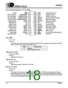
4.0 PIN DESCRIPTION - PCM MODE
Reset
See Description
See Description
See Description
RST
M4(AD0/CS)
M3(AD1/CDIN)
M2(SCL/CCLK)
VREF
FILT+
FILT-
Voltage Reference
Reference Filter
Reference Ground
Common ModeS Voltage
Differential Output
Differential Output
Analog Power
1
2
3
4
5
6
7
8
28
27
26
25
24
23
22
21
20
19
18
17
16
15
CMOUT
AOUTL-
AOUTL+
VA
AGND
AOUTR+
AOUTR-
AGND
MUTEC
C/H
See Description M0(SDA/CDOUT)
Digital Ground
Digital Power
Digital Power
Digital Ground
Master Clock
Serial Clock
Left/Right Clock
Serial Data
See Description
DGND
VD
VD
Analog Ground
DGND
MCLK
SCLK
LRCK
SDATA
M1
Differential Output
Differential Output
Analog Ground
Mute Control
Control port/Hardware select
Soft Mute
9
10
11
12
13
14
MUTE
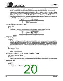
Reset - RST
Pin 1, Input
Function:
The device enters a low power mode and all internal state machines registers are reset when low. When
high, the device will be in a normal operation mode .
DESCRIPTION
RST
Enabled
Normal operation mode
0
1
Digital Ground - DGND
Pins 6 and 9, Inputs
Function:
Digital ground reference.
Digital Power - VD
Pins 7 and 8, Input
Function:
Digital power supply. Typically 5.0 to 3.0 VDC.
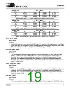
Master Clock - MCLK
Pin 10, Input
Function:
The master clock frequency must be either 256x, 384x, 512x or 768x the input sample rate in Single
Speed Mode; either 128x, 192x 256x or 384x the input sample rate in Double Speed Mode; or 64x, 96x
128x or 192x the input sample rate in Quad Speed Mode. Tables 4-6 illustrate the standard audio sample
rates and the required master clock frequencies.
18
DS333F1

 CIRRUS [ CIRRUS LOGIC ]