CS4397
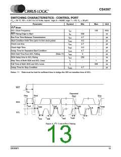
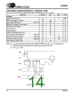
SWITCHING CHARACTERISTICS - CONTROL PORT
(T = 25 °C; VD = 5.25 V to 3.0 Volts; Inputs: logic 0 = AGND, logic 1 = VD, C = 30 pF)
A
L
Parameter
Symbol
Min
Max
Unit
SPI Mode
CCLK Clock Frequency
f
-
6
MHz
ns
ns
µs
ns
ns
ns
ns
ns
ns
ns
ns
sclk
RST Rising Edge to CS Falling
CCLK Edge to CS Falling
CS High Time Between Transmissions
CS Falling to CCLK Edge
CCLK Low Time
t
500
500
1.0
20
66
66
40
15
-
-
srs
(Note 12)
t
-
spi
csh
css
t
t
-
-
t
-
scl
CCLK High Time
t
-
-
sch
CDIN to CCLK Rising Setup Time
CCLK Rising to DATA Hold Time
Rise Time of CCLK and CDIN
Fall Time of CCLK and CDIN
CCLK Falling to CDOUT valid
t
dsu
(Note 13)
(Note 14)
(Note 14)
t
-
dh
t
100
100
r2
t
-
f2
t
45
ov
Notes: 12. t only needed before first falling edge of CS after RST rising edge. t = 0 at all other times.
spi
spi
13. Data must be held for sufficient time to bridge the transition time of CCLK.
14. For F
< 1 MHz
SCK
RST
t
t
srs
CS
t
t
t
spi css
scl
sch
t
csh
CCLK
t
t
r2
f2
CDIN
t
t
dsu
dh
CDOUT
t
ov
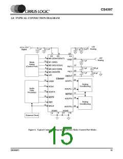
Figure 5. SPI Control Port Timing
14
DS333F1

 CIRRUS [ CIRRUS LOGIC ]