®
4.3.3 Popguard
4.3.3a Power-up
When the device is initially powered-up, the audio outputs, AOUTxx, are clamped to VQ
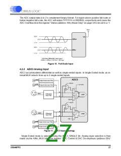
which is initially low. After the RST pin is brought high and MCLK is applied, the outputs
begin to ramp with VQ towards the nominal quiescent voltage. This ramp takes approx-
imately 400 ms to complete. The gradual voltage ramping allows time for the external
DC-blocking capacitors to charge to VQ, effectively blocking the quiescent DC voltage.
Once valid DAC_LRCK, DAC_SCLK and DAC_SDINx are applied, audio output begins
approximately 2000 sample periods later.
4.3.3b Power-down
To prevent audio transients at power-down the DC-blocking capacitors must fully dis-
charge before turning off the power. In order to do this, the PDN bit in register “Power
Control (address 02h)” on page 45 must be set to ‘1’ for a period of about 250 ms before
removing power. During this time, voltage on VQ and the audio outputs discharge grad-
ually to AGND. If power is removed before this 250 ms time period has passed a tran-
sient will occur when the VA supply drops below that of VQ. There is no minimum time
for a power cycle. Power may be re-applied at any time.
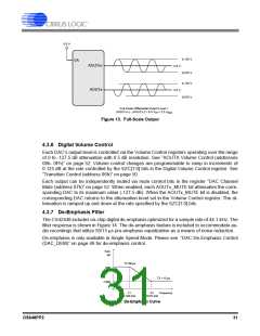
4.3.4 Mute Control
The Mute Control pin, MUTEC, is typically connected to an external mute control circuit. The use
of external mute circuits is not mandatory but may be desired for designs requiring the absolute
minimum in extraneous clicks and pops.
MUTEC is in high impedance mode during power up or when the CS42448 is in power down
mode by setting the PDN bit in the register “Power Control (address 02h)” on page 45 to a ‘1’.
Once out of power-down mode the pin can be controlled by the user via the control port (see
“MUTEC Pin Control (address 1Bh)” on page 55), or automatically asserted to the active state
when zero data is present on all DAC inputs, when all DAC outputs are muted or when serial
port clock errors occur.
To prevent large transients on the output, it is recommended to mute the DAC outputs before
the Mute Control pin is asserted.
4.3.5 Line-level Outputs and Filtering
The CS42448 contains on-chip buffer amplifiers capable of producing line level differential as
well as single-ended outputs on AOUT1-AOUT8. These amplifiers are biased to a quiescent DC
level of approximately VQ.
The delta-sigma conversion process produces high frequency noise beyond the audio pass-
band, most of which is removed by the on-chip analog filters. The remaining out-of-band noise
can be attenuated using an off-chip low pass filter.
See “DAC Output Filter” on page 59 for recommended output filter. The active filter configuration
accounts for the normally differing AC loads on the AOUTx+ and AOUTx- differential output pins.
Also shown is a passive filter configuration which minimizes costs and the number of compo-
nents.
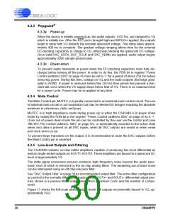
Figure 13 shows the full-scale analog output levels. All outputs are internally biased to VQ, ap-
proximately VA/2.
30
DS648PP2

 CIRRUS [ CIRRUS LOGIC ]