CDB5510/11/12/13
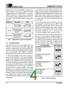
DIP switches on the CDB5510 should be set to the
“CS5511/13 Internally Clocked” section of Table
3.
plifier will be 10 in the single configuration, or 21
in the dual configuration. Different gain values can
be achieved by changing the value of resistors R6,
R17, and R18.
1.6 PC Interface
1.8 Interfacing to an External Controller
The evaluation system comes with software and an
RS-232 cable to link the evaluation board to the
The ADC serial interface is SPI and MICROW-
PC. The executable software was developed with IRETM compatible. The interface control lines (CS,
LabWindows/CVI and meant to run under Win- SDO, and SCLK) are connected to the 8515 micro-
dows 95 or 98. After installing the software, read controller on the CDB5510. The ADCs can be in-
the readme.txt file for any last minute changes in
the software. Additionally, Section 2.0: Software
in this document further details how to install and
use the software.
terfaced to an external microcontroller through
HDR6 on the CDB5510. To accomplish this, the
CDB5510 board must be modified in one of three
ways: 1) remove the microcontroller from its sock-
et, 2) remove resistors R20-R22, or 3) cut the inter-
face control traces between the microcontroller and
the header.
1.7 Adding an Amplifier to the CDB5510
The CDB5510 is laid out so that a standard 8-pin
SOIC dual op-amp of the user’s choosing can be in-
stalled on the board to allow evaluation of the
CS5510/11/12/13’s performance with an op-amp
front-end. If an op-amp front-end is desired, the ad-
ditional components such as feedback resistors and
bypass capacitors must also be installed on the
board. A schematic of the amplifier section includ-
ing some typical component values is shown in
Figure 9. The amplifier is configured to operate in
either a single non-inverting, or a dual differential
configuration. The mode of operation can be select-
ed by changing the jumper on HDR2. Using the
components shown in Figure 9, the gain of the am-
DS337DB2
5

 CIRRUS [ CIRRUS LOGIC ]