CDB5510/11/12/13
1. HARDWARE
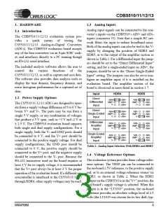
1.3 Analog Inputs
Analog input signals can be connected to the con-
verter’s inputs via the CDB5510’s AIN+ and AIN-
inputs (connector J3). Note that a simple RC net-
work filters the input to reduce broadband noise.
Both of the analog inputs can also be tied to the V-
supply by changing the position of HDR4 and
HDR5, or to the output of the amplifier section as
shown in Table 1. For a differential input the jump-
ers should be set to the “Direct Differential Input”
setting, and for a single-ended input on AIN+, the
jumpers should be set to the “Direct Single-Ended
Input” setting. The jumpers can also be set to con-
figure an amplifier input, if it is installed on the
evaluation board. The amplifier section of the
board is discussed in more detail in section 1.7.
1.1 Introduction
The CDB5510/11/12/13 evaluation system pro-
vides
a
quick means of testing the
CS5510/11/12/13 Analog-to-Digital Converters
(ADCs). The CDB5510 evaluation board accepts
any of the four converters via an 8-pin SOIC sock-
et, and interfaces directly to a PC running though
an RS-232 serial interface.
The included analysis software allows the user to
control
the
various
functions
of
the
CS5510/11/12/13, as well as capture and save data.
The software also provides data analysis tools to
display the time domain, frequency domain, and
noise histogram performance for a captured set of
data.
Input
HDR4
HDR5
1.2 Power Supply Options
Direct
Differential
Input
AIN+
AMP+
V-
AIN-
AMP-
V-
O
O
O
O AIN+
O AIN+
O AIN+
O
O
O
O AIN-
O AIN-
O AIN-
The CS5510/11/12/13 ADCs are designed to oper-
ate from a supply voltage difference of 5 to 6 V be-
tween V+ and V-. The parts may be run from a
single 5 V supply, or any combination of voltages
that produce a 5 V span, such as +3 V and -2 V or
± 2.5 V. The CDB5510 evaluation board supports
both single and dual supply configurations. For a
single supply, both the V- and GND posts should
be connected to 0 V, and the V+ post should be
connected to the positive supply voltage. For dual
supply configurations, the GND post should be
connected to 0 V, the positive supply should be
connected to the V+ post, and the negative supply
should be connected to the V- post. Because the
RS-232 transceiver used on the board requires at
least 3 V for its supply voltage, it is recommended
that the V+ post always be at least 3 V for proper
operation of the evaluation board. If a different mi-
crocontroller is interfaced to the CS5510/11/12/13
through HDR6, other supply voltages may be used.
Direct
Single-Ended
Input
AIN+
AMP+
V-
AIN-
AMP-
V-
O
O
O
O AIN+
O AIN+
O AIN+
O
O
O
O AIN-
O AIN-
O AIN-
Differential
Amplifier
Input
AIN+
AMP+
V-
AIN-
AMP-
V-
O
O
O
O AIN+
O AIN+
O AIN+
O
O
O
O AIN-
O AIN-
O AIN-
Single-Ended
Amplifier
Input
AIN+
AMP+
V-
AIN-
AMP-
V-
O
O
O
O AIN+
O AIN+
O AIN+
O
O
O
O AIN-
O AIN-
O AIN-
Table 1. Analog Input Selection With HDR4 and HDR5
1.4 Voltage Reference Options
The evaluation system provides three voltage refer-
ence options. The VREF pin can be connected to
the on-board 2.5V reference, to the positive supply
rail, or to an external voltage reference source via
HDR3, as shown in Table 2. When the HDR3
jumper on the CDB5510 is in the”V+” position, the
eval board’s supply voltage is selected. When this
jumper is in the “LT1019” position, the on-board
reference provides an absolute voltage level of 2.5
volts (the LT1019 was chosen for its low drift, typ-
DS337DB2
3

 CIRRUS [ CIRRUS LOGIC ]