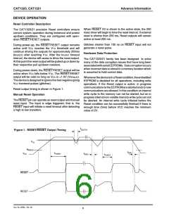
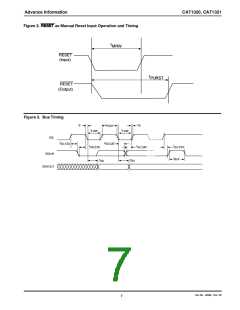
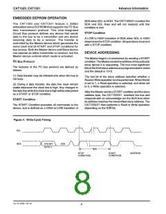
Advance Information
CAT1320, CAT1321
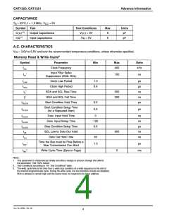
RESET CIRCUIT A.C. CHARACTERISTICS
Test
Conditions
Symbol
Parameter
Min
Typ
Max
Units
tPURST
tRPD
Reset Timeout
Note 2
Note 3
130
200
270
5
ms
µs
VTH to RESET output Delay
tGLITCH
MR Glitch
tMRW
VCC Glitch Reject Pulse Width
Manual Reset Glitch Immunity
MR Pulse Width
Note 4, 5
Note 5
30
ns
ns
µs
100
Note 5
5
POWER-UP TIMING5,6
Test
Conditions
Symbol
Parameter
Min
Typ
Max
Units
tPUR
tPUW
Power-Up to Read Operation
Power-Up to Write Operation
270
270
ms
ms
Notes:
1. Test Conditions according to “AC Test Conditions” table.
2. Power-up, Input Reference Voltage V = V , Reset Output Reference Voltage and Load according to “AC Test Conditions” Table
CC
TH
3. Power-Down, Input Reference Voltage V = V , Reset Output Reference Voltage and Load according to “AC Test Conditions” Table
CC
TH
4.
5. This parameter is characterized initially and after a design or process change that affects the parameter. Not 100% tested.
6. and t are the delays required from the time V is stable until the specified memory operation can be initiated.
V
Glitch Reference Voltage = V ; Based on characterization data
THmin
CC
t
PUR
PUW
CC
AC TEST CONDITIONS
Input pulse voltages
0.2VCC to 0.8VCC
10 ns
Input rise and fall times
Input reference voltages
Output reference voltages
0.3VCC, 0.7VCC
0.5VCC
Current Source: IOL = 3mA;
CL = 100pF
Output Load
RELIABILITY CHARACTERISTICS
Symbol
Parameter
Reference Test Method
Min
Max
Units
Cycles/Byte
Years
(1)
NEND
Endurance
MIL-STD-883, Test Method 1033 1,000,000
(1)
TDR
Data Retention
ESD Susceptibility
Latch-Up
MIL-STD-883, Test Method 1008
MIL-STD-883, Test Method 3015
JEDEC Standard 17
100
2000
100
(1)
VZAP
Volts
(1)(2)
ILTH
mA
Notes:
1. This parameter is tested initially and after a design or process change that affects the parameter. Not 100% tested.
2. Latch-up protection is provided for stresses up to 100mA on input and output pins from -1V to V + 1V.
CC
Doc No. 25085, Rev. 00
5

 CATALYST [ CATALYST SEMICONDUCTOR ]