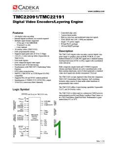
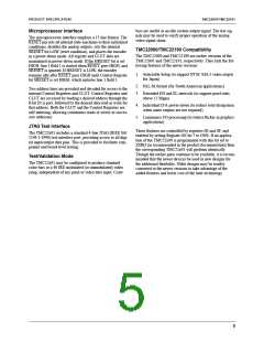
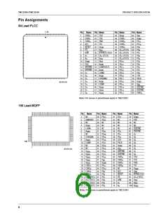
PRODUCT SPECIFICATION
TMC22091/TMC22191
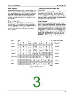
Mask Register
Colorspace Conversion Matrix and
Interpolator
A Mask Register is provided which is logically ANDed with
incoming color-index data to facilitate pixel animation and
other special graphics effects. The Mask Register is ahead of
the Data Key comparators and is enabled only when color-
index input is selected. Mask Register programming and
operation are similar to that of the 171/176 family of graph-
ics RAMDACS.
The matrix converts RGB data (whether from RGB inputs or
color-indexed CLUT data) into Y, B-Y, R-Y format for
encoding. In input configurations where the pixel input is
already inY, B-Y, R-Y format, the matrix is bypassed. When
pixel data is input inYC C 422 format, the interpolation fil-
ters produce YC C 444 for encoding.
B R
B R
Color Lookup Table
Sync Generator
The Color Lookup Table (CLUT) is a 256 x 8 x 3 random-
access memory. It provides means for offset, gain, gamma,
The TMC22x91 can operate in Master, Genlock, or Slave
modes. In Master and Genlock modes, the encoder internally
generates all timing and sync signals, and provides Horizon-
tal Sync, Vertical Sync, and Pixel Data Control (PDC) to the
external frame buffer circuitry. PDC is independently select-
able to function as an input or an output. In Genlock mode,
the TMC22x91 timing is controlled by the TMC22071 Gen-
and color correction in RGB andYC C operating modes. It
B R
provides a full 24-bit color lookup function for color-index
mode. It can be loaded in the same manner as a standard
VGA RAMDAC.
locking Video Digitizer over the CVBS bus, GVSYNC,
7-0
and GHSYNC. The encoder, in turn, produces VHSYNC,
VVSYNC, and PDC for the frame buffer interface.
MODE
Format Control Register
MSB LSB
MSB
23
LSB
0
16 15
G0
8
7
GBR444
00011000
00010000
00011100
00011101
0001X011
G
R
Y
Y
B
R
B
G7
R7
Y7
B
B0 R7
R0
7
RGB444
G
R0 G7
G0 B7
B0
YC C 444
B R
C
C
R
Y0 CB7
CB7
CB0RR7
RR0
B
CB0
CR0
YC C 422
B R
C /C
CR7
Y7
Y0
B R
COLOR INDEX
GBR15
Pixel
P7
B
G
P0
R0
00011010
00010010
G
R
R
G4
G0 B4
R0 G4
B0 R4
RGB15
B
R4
G0 B4
B0
24300A
Figure 1a. Pixel Data Format
3

 CADEKA [ CADEKA MICROCIRCUITS LLC. ]