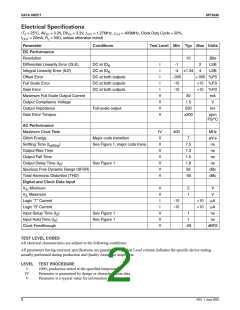
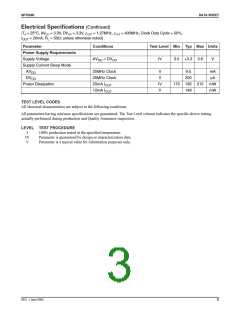
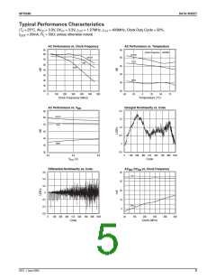
DATA SHEET
SPT5240
I
Sleep
Mode
Select
OUT
Adjust
R
SET
Clock In
CLK
I
PWD
SET
IO
VO
VO
P
P
50Ω
50Ω
10-bit
Data Bus
SPT5240
IO
N
N
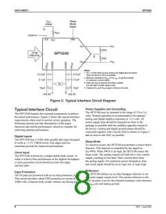
Notes:
1. FB = Ferrite Bead across analog and digital ground planes.
Place as close to DAC as feasible.
0.01µF
0.01µF
2. Minimum resistance (RSET) from ISET to ground relsults
in maximum current output.
0.1µF
0.1µF
3. PWD pin has an internal pull-down resistor.
Set pin high to initate sleep mode.
4. Outputs (IOP and ION) require minimum 5Ω load.
FB
+
+
10µF
10µF
+D3.3V
+A3.3V
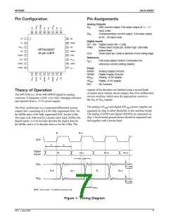
Figure 2: Typical Interface Circuit Diagram
Power Supplies and Grounding
The SPT5240 may be operated in the range of 3.0 to 3.6
Typical Interface Circuit
The SPT5240 requires few external components to achieve
the stated performance. Figure 2 shows the typical interface
requirements when used in normal circuit operation. The
following sections provide descriptions of the major
functions and outline performance criteria to consider for
achieving optimal performance.
volts. Normal operation is recommended to be separate
analog and digital supplies operating at +3.3 volts. All
power supply pins should be bypassed as close to the
package as possible with the smallest capacitor closest to
the device. Analog and digital ground planes should be
connected together with a ferrite bead as shown in Figure 2
and as close to the DAC as possible.
Digital Inputs
The SPT5240 has a 10-bit-wide parallel data input designed
to work at +3.3V CMOS levels. Fast edges and low
transients provide for improved performance.
Sleep Mode
To conserve power, the SPT5240 incorporates a power down
function. This function is controlled by the signal on
pin PWD. When PWD is set high, the SPT5240 enters the
sleep mode. The analog outputs are both set to zero current
output, resulting in less than 10mA current draw from
the analog supply. For minimum power dissipation, data
and clock inputs should be set to logic low or logic high.
Clock Input
The SPT5240 is driven by a single-ended clock circuit. In
order to achieve best performance at the highest throughput,
a clock generation circuit should provide fast edges
and low jitter.
Reference
Input Protection
The SPT5240 utilizes an on-chip bandgap reference to set
full-scale output current level. The current reference to the
DAC circuitry is set by the external resistance value between
All I/O pads are protected with an on-chip protection circuit.
This circuit provides robust ESD protection in excess of
3,000 volts, in human body model, without sacrificing speed.
the I
pin and analog ground.
SET
8
REV. 1 June 2003

 CADEKA [ CADEKA MICROCIRCUITS LLC. ]