SPT5240
DATA SHEET
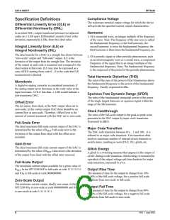
Pin Configuration
Pin Assignments
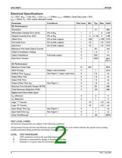
Analog Outputs
IO
DAC current output. Full-scale output at 11…11
P
input code.
IO
Complementary current output. Full-scale output
N
at 00…00 input code.
D2
1
2
3
4
5
6
7
8
24 D8
Digital Inputs
D0 – D9 Digital inputs (D0 = LSB).
D1
DVDD
D0
23 DGND
22
D9
PWD
Power down mode pin. Active high. Internally
pulled down.
Clock input pin. Data is latched on the rising edge.
SPT5240SIT
32-pin LQFP
21 DGND
20 PWD
19 AVDD
18 AGND
17 ISET
CLK
DGND
Reference
CLK
DGND
AGND
I
Full-scale adjust control. Connection for
reference-current setting resistor.
SET
Power
AGND
DGND
Analog Supply Ground.
Digital Supply Ground.
Analog +3.3V supply.
AV
DD
DV
N/C
Digital +3.3V supply.
No Connect
DD
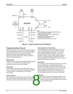
outputs of the decoders are latched using a second bank
of master-slave latches whose outputs then drive differential
current switches, which steer the appropriate current to
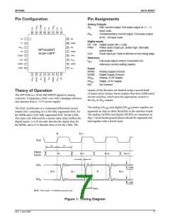
Theory of Operation
The SPT5240 is a 10-bit 400 MWPS digital-to-analog
converter. It integrates a DAC core with a bandgap reference
and operates from a +3.3V power supply.
the IO or IO outputs.
P
N
The analog (AV ) and digital (DV ) power supplies are
DD
DD
The DAC architecture is a compound differential current
output DAC consisting of a 6-bit fully segmented DAC for
the MSBs and a 4-bit fully segmented DAC for the LSBs.
The input cell, followed by a master-slave latch, buffers the
digital inputs. A 6:64 decoder decodes the digital data for
the MSBs, and a 4:16 decoder does so for the LSBs. The
separated on chip to allow flexibility in the interface board.
The analog (AGND) and digital (DGND) are separated on
chip. Circuit board ground planes should be separated and
tied together with a ferrite bead.
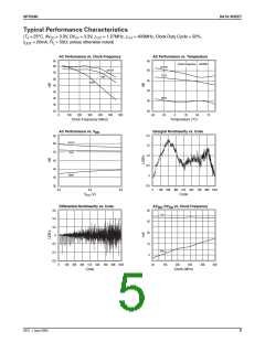
N
N+1
CLK
tS
tH
Digital
Inputs
N
N+1
N+2
N+3
tD
VO
P
1 LSB
N-2
N
N+1
N-1
VO
N
1 LSB
tsettling
NOTE: Not to scale. For definition purposes only.
Figure 1: Timing Diagram
REV. 1 June 2003
7

 CADEKA [ CADEKA MICROCIRCUITS LLC. ]