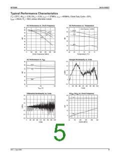
DATA SHEET
SPT5240
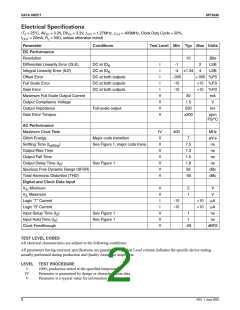
Electrical Specifications
(TA = 25°C, AVDD = 3.3V, DVDD = 3.3V, ƒOUT = 1.27MHz, ƒCLK = 400MHz, Clock Duty Cycle = 50%,
I
= 20mA, R = 50Ω; unless otherwise noted)
OUT
L
Parameter
Conditions
Test Level Min Typ Max Units
DC Performance
Resolution
10
Bits
LSB
LSB
Differential Linearity Error (DLE)
Integral Linearity Error (ILE)
Offset Error
DC at IO
DC at IO
I
I
-1
-4
2
4
N
1.34
N
DC at both outputs
DC at both outputs
DC at both outputs
I
-.005
-15
-15
+.005 %FS
+15 %FS
+15 %FS
mA
Full Scale Error
I
Gain Error
I
Maximum Full Scale Output Current
Output Compliance Voltage
Output Impedance
V
V
V
V
30
1.5
V
Full-scale output
250
300
kΩ
Gain Error Tempco
ppm
FS/°C
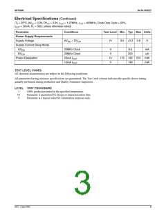
AC Performance
Maximum Clock Rate
Glitch Energy
IV
V
V
V
V
V
V
V
400
MHz
pV-s
ns
Major code transition
7
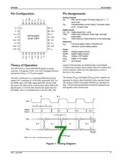
Settling Time (t
)
See Figure 1, major code trans.
7.5
1.3
1.5
1.8
58
settling
Output Rise Time
Output Fall Time
ns
ns
Output Delay Time (t )
See Figure 1
ns
D
Spurious Free Dynamic Range (SFDR)
Total Harmonic Distortion (THD)
Digital and Clock Data Input
dBc
dBc
-55
V
Minimum
V
V
I
2
1
V
V
IH
V Maximum
IL
Logic “1” Current
Logic “0” Current
-10
-10
+10
+10
µA
µA
I
Input Setup Time (t )
See Figure 1
See Figure 1
V
V
V
1
1
ns
S
Input Hold Time (t )
ns
H
Clock Feedthrough
-29
dBFS
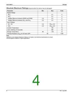
TEST LEVEL CODES
All electrical characteristics are subject to the following conditions:
All parameters having min/max specifications are guaranteed. The Test Level column indicates the specific device testing
actually performed during production and Quality Assurance inspection.
LEVEL TEST PROCEDURE
I
IV
V
100% production tested at the specified temperature.
Parameter is guaranteed by design or characterization data.
Parameter is a typical value for information purposes only.
2
REV. 1 June 2003

 CADEKA [ CADEKA MICROCIRCUITS LLC. ]