Data Sheet
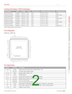
Ordering Information (TQFP-64 Package)
Part Number
Speed
Package
TQFP-64
TQFP-64
TQFP-64
TQFP-64
TQFP-64
TQFP-64
TQFP-64
TQFP-64
Pb-Free RoHS Compliant Operating Temperature Range Packaging Method
CDK2307AITQ64
CDK2307AITQ64X
CDK2307BITQ64
CDK2307BITQ64X
CDK2307CITQ64
CDK2307CITQ64X
CDK2307DITQ64
CDK2307DITQ64X
20MSPS
20MSPS
40MSPS
40MSPS
65MSPS
65MSPS
80MSPS
80MSPS
Yes
Yes
Yes
Yes
Yes
Yes
Yes
Yes
Yes
Yes
Yes
Yes
Yes
Yes
Yes
Yes
-40°C to +85°C
-40°C to +85°C
-40°C to +85°C
-40°C to +85°C
-40°C to +85°C
-40°C to +85°C
-40°C to +85°C
-40°C to +85°C
Tray
Tape & Reel
Tray
Tape & Reel
Tray
Tape & Reel
Tray
Tape & Reel
Moisture sensitivity level for all parts is MSL-2A.
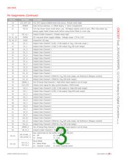
Pin Configuration
QFN-64, TQFP-64
1
2
3
4
5
6
48
47
46
45
44
43
42
41
40
39
38
37
36
35
34
33
CDK2307
7
CLK_EXT
QFN-64, TQFP-64
8
9
10
11
12
13
14
15
16
DVSSCLK
DVDDCLK
CLKP
CLKN
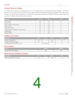
Pin Assignments
Pin No.
1, 18, 23
2
Pin Name
Description
DVDD
CM_EXT
AVDD
Digital and I/O-ring pre driver supply voltage, 1.8V
Common Mode voltage output
3, 9, 12
4, 5, 8
6, 7
Analog supply voltage, 1.8V
AVSS
Analog ground
IP0, IN0
IP1, IN1
DVSSCLK
DVDDCLK
CLKP
Analog input Channel 0 (non-inverting, inverting)
Analog input Channel 1 (non-inverting, inverting)
Clock circuitry ground
10, 11
13
14
Clock circuitry supply voltage, 1.8V
15
Clock input, non-inverting (Format: LVDS, PECL, CMOS/TTL, Sine Wave)
Clock input, inverting. For CMOS input on CLKP, connect CLKN to ground
Digital circuitry ground
16
CLKN
17, 64
DVSS
©2009 CADEKA Microcircuits LLC
www.cadeka.com
2

 CADEKA [ CADEKA MICROCIRCUITS LLC. ]