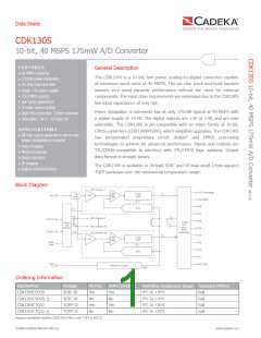
Data Sheet
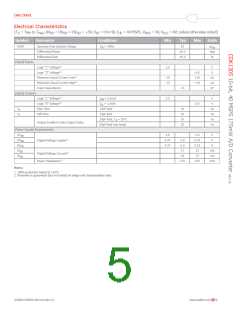
Electrical Characteristics
(T = T to T , AV = DV = OV = +5V, V = 0 to 4V, ƒ = 40 MSPS, V
= 4V, V
= 0V; unless otherwise noted)
Min
A
Max
DD
DD
DD
IN
clk
RHS
RLS
symbꢀꢁ
pꢂꢃꢂmꢄꢅꢄꢃ
cꢀꢆdꢇꢅꢇꢀꢆꢈ
Mꢇꢆ
tyꢉ
Mꢂx
uꢆꢇꢅꢈ
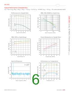
SFDR
Spurious Free Dynamic Range
Differential Phase
ƒIN = 1MHz
63
pspp
deg
%
±0.3
±0.3
Differential Gain
Digital Inputs
Logic “1“ Voltage(1)
2.0
V
Logic “0“ Voltage(1)
Maximum Input Current Low(1)
Maximum Input Current High(1)
0.8
+10
+10
V
-10
-10
μA
μA
pF
Input Capacitance
+5
Digital Outputs
Logic “1“ Voltage(1)
Logic “0“ Voltage(1)
Rise Time
IOH = 0.5mA
IOL = 1.6mA
15pF load
3.5
V
0.4
V
TR
TF
10
10
10
22
ns
ns
ns
ns
Fall Time
15pF load
20pF load, TA = 25°C
50pF load over temp
Output Enable to Data Output Delay
Power Supply Requirements
OVDD
3.0
5.0
5.25
5.25
22
V
V
Digital Voltage Supply(2)
DVDD
AVDD
AIDD
DIDD
4.75
4.75
5.0
5.0
17
V
mA
mA
mW
Digital Voltage Current(1)
Power Dissipation(1)
18
23
175
225
nꢀꢅꢄꢈ:
1. 100% production tested at +25°C.
2. Parameter is guaranteed (but not tested) by design and characterization data.
©2008 CADEKA Microcircuits LLC
www.cadeka.com
5

 CADEKA [ CADEKA MICROCIRCUITS LLC. ]