Data Sheet
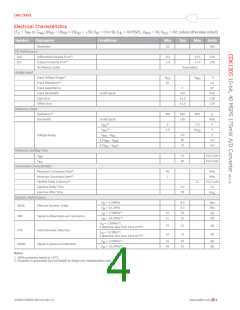
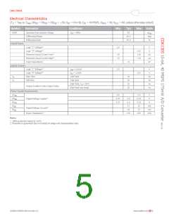
Electrical Characteristics
(T = T to T , AV = DV = OV = +5V, V = 0 to 4V, ƒ = 40 MSPS, V
= 4V, V
= 0V; unless otherwise noted)
Min
A
Max
DD
DD
DD
IN
clk
RHS
RLS
symbꢀꢁ
pꢂꢃꢂmꢄꢅꢄꢃ
cꢀꢆdꢇꢅꢇꢀꢆꢈ
Mꢇꢆ
tyꢉ
Mꢂx
uꢆꢇꢅꢈ
Resolution
10
bits
DC Performance
DLE
ILE
Differential Linearity Error(1)
Integral Linearity Error(1)
No Missing Codes
-0.5
-1.0
+0.5
+1.0
LSB
LSB
Guaranteed
Analog Input
Input Voltage Range(1)
Input Resistance(2)
Input Capacitance
Input Bandwidth
Gain Error
VRLS
50
VRHS
V
kΩ
5
pF
Small Signal
Small Signal
250
MHz
LSB
LSB
±2.0
±2.0
Offset Error
Reference Input
Resistance(1)
300
500
150
600
Ω
MHz
V
Bandwidth
(2)
VRLS
0
2.0
(2)
VRHS
3.0
AVDD
V
VRHS –VRLS
4.0
90
75
V
Voltage Range
Δ (VRHF –VRHS
)
mV
mV
Δ (VRLS –VRLF
)
Reference Settling Time
VRHS
VRLS
15
20
CLK Cycle
CLK Cycle
Conversion Characteristics
Maximum Conversion Rate(1)
40
2
MHz
MHz
Minimum Conversion Rate(2)
Pipeline Delay (Latency)(2)
Aperture Delay Time
12
CLK Cycle
ns
4.0
30
Aperture Jitter Time
pspp
Dynamic Performance
ƒIN = 3.58MHz
ƒIN = 10.3MHz
ƒIN = 3.58MHz(1)
ƒIN = 10.3MHz(1)
8.5
8.3
54
Bits
Bits
dB
ENOB
SNR
Effective Number of Bits
52
51
Signal-to-Noise Ratio w/o Harmonics
Total Harmonic Distortion
52
dB
ƒIN = 3.58MHz(1)
9 distortion bins from 1024 pt FFT
,
55
52
61
53
dB
dB
THD
ƒIN = 10.3MHz(1)
,
9 distortion bins from 1024 pt FFT
ƒIN = 3.58MHz(1)
ƒIN = 10.3MHz(1)
51
49
54
52
dB
dB
SINAD
Signal-to-Noise and Distortion
nꢀꢅꢄꢈ:
1. 100% production tested at +25°C.
2. Parameter is guaranteed (but not tested) by design and characterization data.
©2008 CADEKA Microcircuits LLC
www.cadeka.com
4

 CADEKA [ CADEKA MICROCIRCUITS LLC. ]