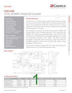
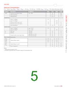
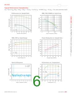
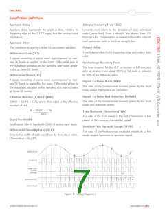
Data Sheet
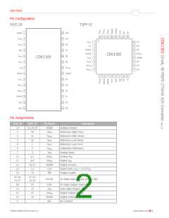
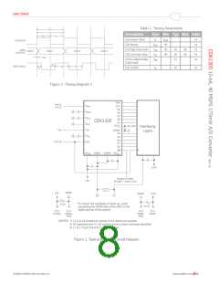
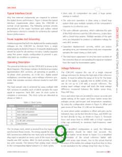
Pin Configuration
SOIC-28
TQFP-32
CDK1305
CDK1305
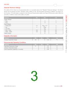
Pin Assignments
SOIC-28
TQFP-32
Pin Name
Description
1,8
2
3,4,28,29
AGND
VRHF
VRHS
VRLS
VRLF
VCAL
VIN
Analog Ground
30
31
32
1
Reference High Force
Reference High Sense
Reference Low Sense
Reference Low Force
Calibration Reference
Analog Input
3
5
6
9
5
7
2
10
11
12
13
15
6,7
8,9
10,11
12
14
AVDD
DVDD
DGND
CLK
Analog VDD
Digital VDD
Digital Ground
Input Clock ƒCLK = FS (TTL)
Output Enable
EN
16-20,
23-27
15-19,
22-26
D0-D9
Tri-State Data Output, (D0 = LSB)
28
14
22
21
4
27
13
21
20
–
D10
DAV
Tri-State Output Overrange
Data Valid Output
OVDD
OGND
N/C
Digital Output Supply
Digital Output Ground
No Connect
©2008 CADEKA Microcircuits LLC
www.cadeka.com
2

 CADEKA [ CADEKA MICROCIRCUITS LLC. ]