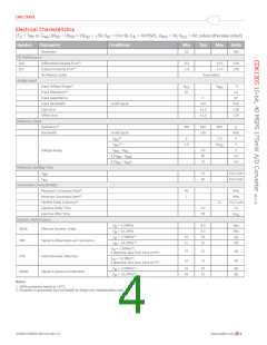
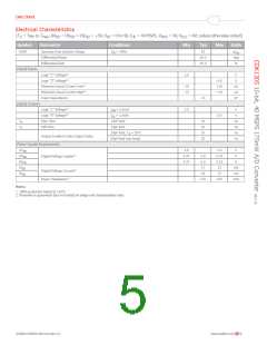
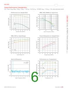
Data Sheet
n
n
ꢀ
Since only 16 comparators are used, a huge power
savings is realized.
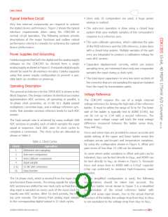
Typical Interface Circuit
Very few external components are required to achieve
the stated device performance. Figure 2 shows the typical
interface requirements when using the CDK1305 in
normal circuit operation. The following sections provide
descriptions of the major functions and outline critical
performance criteria to consider for achieving the optimal
device performance.
ꢀ
The auto-zero operation is done using a closed loop
system that uses multiple samples of the comparator’s
response to a reference zero.
n
ꢀ
The auto-calibrate operation, which calibrates the gain
of the MSB reference and the LSB reference, is also done
with a closed loop system. Multiple samples of the gain
error are integrated to produce a calibration voltage for
each ADC section.
Power Supplies And Grounding
Cadekasuggeststhatboththedigitalandtheanalogsupply
voltages on the CDK1305 be derived from a single
analogsupplyasshowninFigure2.Aseparatedigitalsupply
should be used for all interface circuitry. Cadeka suggests
using this power supply configuration to prevent a pos-
sible latch-up condition on powerup.
n
ꢀ
Capacitive displacement currents, which can induce
sampling error, are minimized since only one comparator
samples the input during a clock cycle.
n
ꢀ
The total input capacitance is very low since sections of
theconverterthatarenotsamplingthesignalareisolated
from the input by transmission gates.
Operating Description
The general architecture for the CMOS ADC is shown in the
Block Diagram. The design contains 16 identical successive
approximation ADC sections, all operating in parallel, a
16-phase clock generator, an 11-bit 16:1 digital output
multiplexer, correction logic, and a voltage reference gen-
erator that provides common reference levels for each ADC
section.
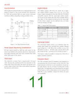
Voltage Reference
The CDK1305 requires the use of a single external
voltage reference for driving the high side of the reference
ladder. It must be within the range of 3V to 5V. The lower
side of the ladder is typically tied to AGND (0.0V), but
can be run up to 2.0V with a second reference. The
analog input voltage range will track the total voltage
difference measured between the ladder sense lines,
The high sample rate is achieved by using multiple SAR
ADC sections in parallel, each of which samples the input
signal in sequence. Each ADC uses 16 clock cycles to
complete a conversion. The clock cycles are allocated as
shown in Table 2.
V
and V
.
RHS
RLS
Force and sense taps are provided to ensure accurate and
stable setting of the upper and lower ladder sense line
voltages across part-to-part and temperature variations.
By using the configuration shown in Figure 4, offset and
gain errors of less than ±2 LSB can be obtained.
Table 2. Clock Cycles
cꢁꢀꢋk
oꢉꢄꢃꢂꢅꢇꢀꢆ
Reference zero sampling
1
2
In cases where wider variations in offset and gain can be
Auto-zero comparison
Auto-calibrate comparison
Input sample
tolerated, V
can be tied directly to V , and AGND can
RHF
REF
3
be tied directly to V
as shown in Figure 5. Decouple
RLF
4
force and sense lines to AGND with a 0.01μF capacitor
(chip cap preferred) to minimize high-frequency noise
injection.
5-15
16
11-bit SAR conversion
Data transfer
If this simplified configuration is used, the following
considerations should be taken into account. The
reference ladder circuit shown in Figure 5 is a simplified
representation of the actual reference ladder with
force and sense taps shown. Due to the actual internal
The 16-phase clock, which is derived from the input clock,
synchronizes these events. The timing signals for adjacent
ADC sections are shifted by one clock cycle so that the an-
alog input is sampled on every cycle of the input clock by
exactly one ADC section. After 16 clock periods, the tim-
ing cycle repeats. The latency from analog input sample
to the corresponding digital output is 12 clock cycles.
structure of the ladder, the voltage drop from V
to V
RHS
RHF
is not equivalent to the voltage drop from V
to V
.
RLF
RLS
©2008 CADEKA Microcircuits LLC
www.cadeka.com
9

 CADEKA [ CADEKA MICROCIRCUITS LLC. ]