Data Sheet
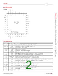
Pin Configuration
QFN-40
DVDD
CM_EXT
AVDD
AVDD
IP
D_7
1
2
30
29
28
27
26
25
24
23
22
21
D_6
D_5
3
CLK_EXT
OVDD
OVDD
ORNG
D_4
4
CDK1307
5
QFN-40
IN
6
AVDD
DVDDCLK
CLKP
7
8
D_3
9
CLKN
D_2
10
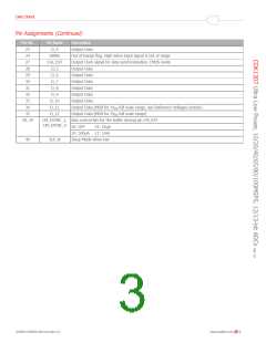
Pin Assignments
Pin No.
Pin Name
Description
0
Ground connection for all power domains. Exposed pad
Digital and I/O-ring pre driver supply voltage, 1.8V
Common Mode voltage output
VSS
1, 11, 16
DVDD
2
3, 4, 7
5, 6
8
CM_EXT
AVDD
Analog supply voltage, 1.8V
IP, IN
Analog input (non-inverting, inverting)
DVDDCLK
Clock circuitry supply voltage, 1.8V
9
Clock input, non-inverting (format: LVDS, LVPECL, CMOS/TTL, Sine Wave)
Clock input, inverting. For CMOS input on CLKP, Connect CLKN to ground
CLKP
CLKN
10
12
CLK_EXT_EN CLK_EXT signal enabled when low (zero). Tristate when high.
13
DFRMT
PD_N
Data format selection. 0: Offset Binary, 1: Two's Complement
14
Full chip Power Down mode when Low. All digital outputs reset to zero. After chip power up
always apply Power Down mode before using Active Mode to reset chip.
15
OE_N
OVDD
Output Enable. Tristate when high
17, 18, 25,
26, 36, 37
I/O ring post-driver supply voltage. Voltage range 1.7 to 3.6V
19
20
21
22
D_0
D_1
D_2
D_3
Output Data (LSB, 13-bit output or 1Vpp full scale range)
Output Data (LSB, 12-bit output 2Vpp full scale range)
Output Data
Output Data
©2009 CADEKA Microcircuits LLC
www.cadeka.com
2

 CADEKA [ CADEKA MICROCIRCUITS LLC. ]