High-Speed Response Non-Isolated POL DC-DC Converter
4A/9.5A BSV-M Series
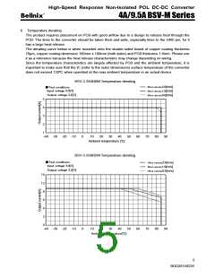
7. Outer dimensions and description of pins
7-1 Shape and dimensions (SMD type)
20.32
15.24
8.89
3.81 (1.90)
3.81±0.2
3.81±0.2
6.35±0.2
ピックアップ
Pickup p位os置ition
1 Pin Mark
1.27±0.2
1ピンマーク
1.27±0.2
(5) (4)
(2) (1)
管理密番
(3)
(1)
Production code for control
IC
Company Logo
会社ロゴ表示
(6) (7)
(8)
3.81±0.2
1.27±0.2
(1.90)
Lot No.
Model name
(1.90)
(7.25)
ロット表示
型名表示
3.18±0.2
16.50
(12.78)
24.0
5.40
Top View
Bottom View
Side View
Unit: mm
・Dimensional tolerance (unless specified) ±0.5
・Weight = 2.3g typ.
・Lot No. display: (1)(2)(3)
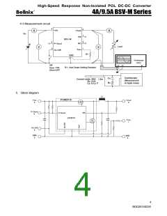
Pin Function
1
2
3
4
5
6
7
8
Trim
+Vout
GND
+Vin
On/Off
P-Good
HS
(1) The last digit of A.D.
(2)Manufacturing month (Oct/Nov/Dec = O/N/D)
(3) Production code (may not be indicated)
・Pin’s variation is 0.2 mm max. (when placed on
the level).
NC
7-2 Recommended footprint dimensions
20.32
Converter mounting
15.24
8.89
3.81
position
コンバータ実装位置
内部はパターン禁止
*1 To form via on the HS (Heat
No patterns inside
Via prohibited area
ビア発生禁止領域
Spreader)
following area.
footprint,
use
the
1.5
4.1 6.6
1.5
4.1
HS部のビア形成可能領域
Refer to Note (*1)
<Example of via
formation>
Through hole of
は注記(※1)を参照
for area allowed for
via in HS part
0.4
×6
drill dia. ɸ0.4 x 6
1.0
1.0
Via formable area
※1
4.1
1.5
(1.9)
3.4
HS footprint
HS
5.40
16.50
(24.0)
Note) Recommended dimensions are shown above. Use your design standard for your specific
design.
6
BDD20150226

 BELLNIX [ Bellnix ]