High-Speed Response Non-Isolated POL DC-DC Converter
4A/9.5A BSV-M Series
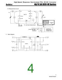
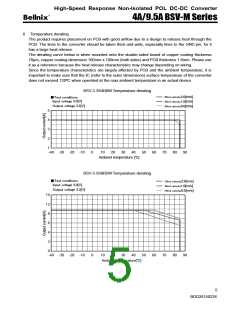
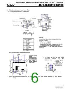
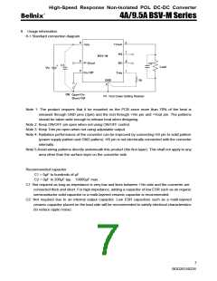
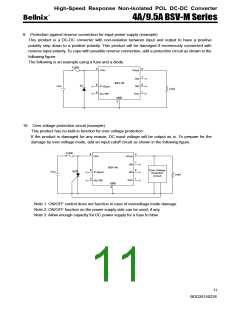
8. Usage information
8-1 Standard connection diagram
4
2
+Vout
+Vin
7
8
HS
NC
BSV-M
6
5
P-Good
On/Off
C2
C1
+
Load
Vin
1
Trim
GND
R1
3
SW
Open=On
Short=Off
R1: Vout Down設定抵抗
R1: Vout Down Setting Resistor
Note 1: The product requires that it be mounted on the PCB since more than 70% of the heat is
released through GND pins (3pin) and the rest through +Vin pin and +Vout pin. The patterns
should be taken wide enough to release heat when designing.
Note 2: Keep ON/OFF pin open when not using ON/OFF control.
Note 3: Keep Trim pin open when not using adjustable output.
Note 4: Radiation performance of the converter can be improved by connecting HS pin to solid pattern
(power supply pattern and GND pattern). HS pin is not electrically connected with the converter
internally.
Note 5:Avoid wiring patterns directly underneath this product (the first layer). This shall not apply to any
area other than the surface layer on the converter side.
Recommended capacitor
C1 = 0μF to hundreds of μF
C2 = 0μF to 200μF typ. 10000μF max.
C1: Not required as long as impedance is very low and lines between +Vin side and the converter are
connected thick and short. For high impedance, adding a capacitor of low ESR such as an organic
semiconductor solid capacitor or a multi-layered ceramic capacitor is recommended.
C2: Not required due to an internal output capacitor. Low ESR capacitors such as a multi-layered
ceramic capacitor placed on the load side will be recommended to satisfy electrical characteristics
(to reduce ripple noise).
7
BDD20150226

 BELLNIX [ Bellnix ]