BL9110
1A Low Dropout, Low Quiescent Current
High PSRR CMOS Linear Regulator
depending on the ESR of the output
capacitor. Increasing the output capacitor's
value and decreasing the ESR attenuates
the overshoot.
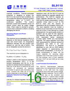
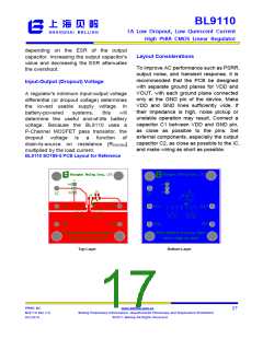
Layout Considerations
To improve AC performance such as PSRR,
output noise, and transient response, it is
recommended that the PCB be designed
with separate ground planes for VDD and
VOUT, with each ground plane connected
only at the GND pin of the device. Make
VDD and GND lines sufficiently wide. If
their impedance is high, noise pickup or
unstable operation may result. Connect a
capacitor C1 between VDD and GND pin,
as close as possible to the pins. Set
external components, especially the output
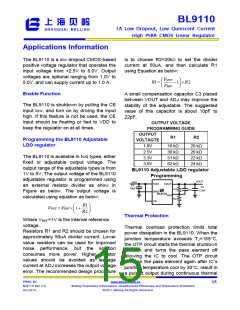
Input-Output (Dropout) Voltage
A regulator's minimum input-output voltage
differential (or dropout voltage) determines
the lowest usable supply voltage. In
battery-powered
systems,
this
will
determine the useful end-of-life battery
voltage. Because the BL9110 uses a
P-Channel MOSFET pass transistor, the
dropout voltage is
a
function of
capacitor C2, as close as possible to the IC,
and make wiring as short as possible.
drain-to-source on resistance [RDS(ON)
multiplied by the load current.
]
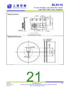
BL9110 SOT89-5 PCB Layout for Reference
Top Layer
Bottom Layer
PPMIC BU
BL9110 Rev 2.0
04/2016
www.belling.com.cn
17
Belling Proprietary Information. Unauthorized Photocopy and Duplication Prohibited
© 2011 Belling All Rights Reserved

 BELLING [ BELLING ]