BL9110
1A Low Dropout, Low Quiescent Current
High PSRR CMOS Linear Regulator
Applications Information
The BL9110 is a low dropout CMOS-based
positive voltage regulator that operates the
input voltage from +2.5V to 6.0V. Output
voltages are optional ranging from 1.0V to
5.0V, and can supply current up to 1.0 A.
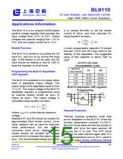
is to choose R2=20kΩ to set the divider
current at 50uA, and then calculate R1
using Equation as below:
VOUT
R1
1 R2
VREF
Enable Function
A small compensation capacitor C3 placed
between VOUT and ADJ may improve the
stability of the adjustable. The suggested
value of this capacitor is about 10pF to
22pF.
The BL9110 is shutdown by pulling the CE
input low, and turn on by driving the input
high. If this feature is not be used, the CE
input should be floating or tied to VDD to
keep the regulator on at all times.
OUTPUT VOLTAGE
PROGRAMMING GUIDE
OUTPUT
R1
R2
Programming the BL9110 Adjustable
LDO regulator
VOLTAGTE
1.8V
16 kΩ
30 kΩ
51 kΩ
62 kΩ
20 kΩ
20 kΩ
22 kΩ
24 kΩ
2.5V
The BL9110 is available in two types, either
fixed or adjustable output voltage. The
output range of the adjustable types is from
1V to 5V. The output voltage of the BL9110
adjustable regulator is programmed using
an external resistor divider as show in
Figure as below. The output voltage is
calculated using equation as below:
3.3V
3.6V
BL9110 Adjustable LDO regulator
Programming
VOUT
VDD
VDD
VOUT
C1
10uF
C2
2.2uF
R1
R2
C3
GND
BL9110
ADJ
CE
R1
V
OUT VREF 1
R2
Thermal Protection
Where VREF=1V is the internal reference
voltage.
Thermal overload protection limits total
power dissipation in the BL9110. When the
junction temperature exceeds TJ=165°C ,
the OTP circuit starts the thermal shutdown
function and turns the pass element off
allowing the IC to cool. The OTP circuit
turns on the pass element again after IC’s
junction temperature cool by 30°C , result in
a pulsed output during continuous thermal
Resistors R1 and R2 should be chosen for
approximately 50uA divider current. Lower
value resistors can be used for improved
noise performance, but the solution
consumes more power. Higher resistor
values should be avoided as leakage
current at ADJ increases the output voltage
error. The recommended design procedure
PPMIC BU
BL9110 Rev 2.0
04/2016
www.belling.com.cn
15
Belling Proprietary Information. Unauthorized Photocopy and Duplication Prohibited
© 2011 Belling All Rights Reserved

 BELLING [ BELLING ]