BL9110
1A Low Dropout, Low Quiescent Current
High PSRR CMOS Linear Regulator
overload conditions. Thermal-overloaded
protection is designed to protect the
BL9110 in the event of fault conditions. Do
not exceed the absolute maximum junction
temperature rating of TJ=125°C for
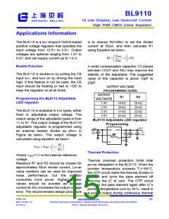
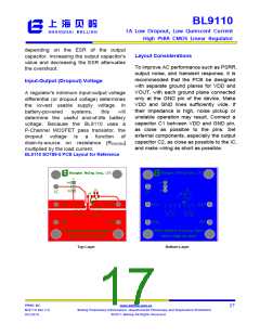
capacitors used with the BL9110 must be
carefully selected for regulator stability and
performance. The BL9110 requires an
output capacitor between the VOUT and
GND pins for phase compensation. Using a
capacitor whose value is ≥1μF on the
BL9110 input and the amount of
capacitance can be increased without limit.
The input capacitor must be located a
distance of not more than 0.5 inch from the
input pin of the IC and returned to a clean
analog ground. Any good quality ceramic or
tantalum can be used for this capacitor.
The capacitor with larger value and lower
continuous
operation.
The
build-in
fold-back current limit protection circuit will
reduce current value as output voltage
drops. When output is shorted to ground,
current limit is reduced to 250mA, avoiding
damaging the device.
Operating Region and Power
Dissipation
ESR
(equivalent
series
resistance)
The maximum power dissipation of BL9110
depends on the thermal resistance of the
case and circuit board, the temperature
difference between the die junction and
ambient air, and the rate of airflow. The
power dissipation across the device is
provides better PSRR and line-transient
response. The output capacitor must meet
both requirements for minimum amount of
capacitance and ESR in all LDO
applications. The BL9110 is designed
specifically to work with low ESR ceramic
output capacitor in space-saving and
performance consideration. In the BL9110,
phase compensation is made with the
output capacitor for securing stable
operation even if the load current is varied.
For this purpose, use a 2.2uF capacitor
between VOUT pin and GND pin as close
as possible.
PD = (VDD−VOUT) ×IOUT + VDD×I Q
The maximum power dissipation is:
PD (MAX) = (TJ (MAX) − TA) /θJA
Where TJ (MAX) is the maximum operation
junction temperature 125°C, TA is the
ambient temperature and the θJA is the
junction to ambient thermal resistance. The
GND pin of the BL9110 performs the dual
function of providing an electrical
connection to ground and channeling heat
away. Connect the GND pin to ground
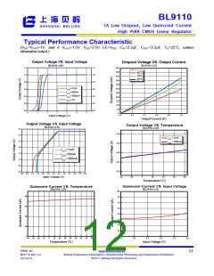
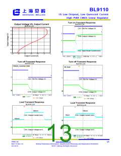
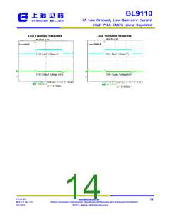
Load-Transient Considerations
The BL9110 load-transient response
graphs show two components of the output
response: a DC shift from the output
impedance due to the load current change,
and the transient response. The DC shift is
quite small due to the excellent load
regulation of the IC. Typical output voltage
transient spike for a step change in the load
current from 0mA to 50mA is tens of mV,
using a large pad or ground plane.
Capacitor Selection and Regulator
Stability
Like any low-dropout regulator, the external
PPMIC BU
BL9110 Rev 2.0
04/2016
www.belling.com.cn
16
Belling Proprietary Information. Unauthorized Photocopy and Duplication Prohibited
© 2011 Belling All Rights Reserved

 BELLING [ BELLING ]