Preliminary Datasheet
BOOST CONTROLLER
AP3039
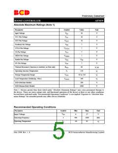
Absolute Maximum Ratings (Note 1)
Parameter
Symbol
Value
Unit
Input Voltage
VIN
30
V
VCC Pin Voltage
VCC
VOUT
VFB
10
V
V
V
V
V
V
V
V
OUT Pin Voltage
10
Feedback Pin Voltage
7
UVLO Pin Voltage
VUVLO
VCS
VSHDN
VEN
7
CS Pin Voltage
7
SHDN Pin Voltage
7
VIN
Enable Pin Voltage
OV Pin Voltage
VOV
7
oC/W
oC
Thermal Resistance (Junction to Ambient, no Heat sink)
Operating Junction Temperature
Storage Temperature Range
Lead Temperature (Soldering, 10sec)
RθJA
TJ
60
150
oC
TSTG
TLEAD
-65 to 150
260
oC
V
ESD (Machine Model)
200
ESD (Human Body Model)
2000
V
Note 1: Stresses greater than those listed under "Absolute Maximum Ratings" may cause permanent damage to
the device. These are stress ratings only, and functional operation of the device at these or any other conditions
beyond those indicated under "Recommended Operating Conditions" is not implied. Exposure to "Absolute Max-
imum Ratings" for extended periods may affect device reliability.
Recommended Operating Conditions
Parameter
Symbol
Min
6
Max
27
Unit
V
V
Input Voltage
Operating Frequency
IN
f
400
1000
kHz
oC
Operating Temperature
May 2008 Rev. 1. 0
TA
-40
85
BCD Semiconductor Manufacturing Limited
5

 BCDSEMI [ BCD SEMICONDUCTOR MANUFACTURING LIMITED ]