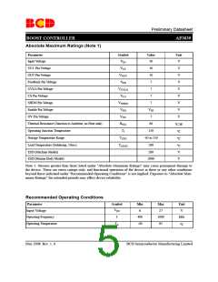
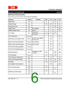
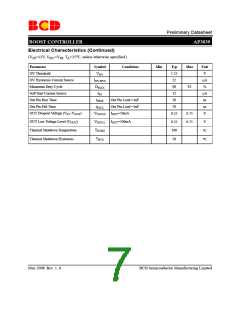
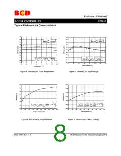
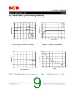
Preliminary Datasheet
BOOST CONTROLLER
AP3039
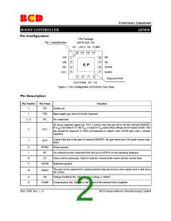
Pin Configuration
FN Package
QFN-3x3-16)
Pin 1 Identification
(
OV UVLO SS COMP
16 15 14 13
EN
NC
1
2
12
11
VIN
NC
FB
E P
SHDN
AGND
3
4
10
9
VCC
5
6
7
8
Exposed PAD
OUTPGND RT CS
Figure 2. Pin Configuration of AP3039 (Top View)
Pin Description
Pin Number
Pin Name
Function
1
EN
VIN
NC
Enable pin
2
Input supply pin, must be locally bypassed
No connection
3, 12
6V linear regulator output pin. VCC is used to bias the gate driver for the external MOSFET.
If VIN is less than 8.5V, the VCC is equal to VIN minus drop voltage across bypass switch. This
4
VCC
pin should be bypassed to GND (recommend to connect with AGND pin) with a ceramic
capacitor
Connect this pin to the gate of external MOSFET, the gate driver has 0.6A peak current capa-
bility
5
OUT
6
7
8
9
PGND
RT
Power ground
An external resistor connected from this pin to GND to set the operating frequency
Sense switch current pin, which is used for current mode control and for current limit
Reference ground
CS
AGND
This pin can be connected to current matched chip and receives error signal used to shut down
the system
10
SHDN
11
13
FB
Voltage Feedback Pin. The reference voltage is 500mV
COMP
Compensation Pin. This pin is the output of the internal Error Amplifier
May 2008 Rev. 1. 0
BCD Semiconductor Manufacturing Limited
2

 BCDSEMI [ BCD SEMICONDUCTOR MANUFACTURING LIMITED ]