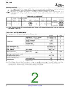
TSC2005
www.ti.com
SBAS379–DECEMBER 2006
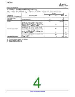
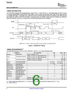
TIMING INFORMATION
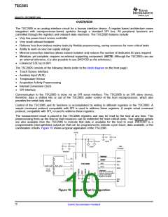
The TSC2005 supports SPI programming in mode CPOL = 0 and CPHA = 0. The falling edge of SCLK is used
to change output (MISO) data and the rising edge is used to latch input (MOSI) data. Eight SCLKs are required
to complete the Byte 1 command cycle, and 24 SCLKs are required for the Byte 0 command cycle. CS can stay
low during the entire 24 SCLKs of a Byte 0 command cycle, or multiple mixed cycles of reading and writing of
bytes and register accesses, as long as the corresponding addresses are supplied.
CS (SS)
tC(SCLK)
tWH(SCLK)
tWH(CS)
tSU(SCLKF-CSR)
tSU(CSF-SCLK1R)
tF
tR
tWL(SCLK)
SCLK
tH(SCLKF-SDOVALID)
BIT 1
tDIS(CSR-SDOZ)
SDO (MISO)
MSB OUT
BIT 0
BIT 0
tD(CSF-SDOVALID)
tSU(SDI-SCLKR)
tH(SDI-SCLKR)
SDI (MOSI)
BIT 1
MSB IN
NOTE: CPOL = 0, CPHA = 0, Byte 0 cycle requires 24 SCLKs, and Byte 1 cycle requires 8 SCLKs.
Figure 1. Detailed I/O Timing
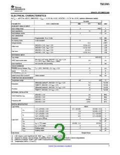
TIMING REQUIREMENTS(1)
All specifications typical at –40°C to +85°C, SNSVDD = I/OVDD = 1.6V, unless otherwise noted.
PARAMETER
Reset low time
TEST CONDITIONS
I/OVDD = SNSVDD ≥ 1.6V(2)
MIN
10
MAX
UNIT
µs
tWL(RESET)
tC(SCLK)
I/OVDD ≥ 1.6V and < 2.7V, 40% to 60% duty cycle
I/OVDD ≥ 2.7V and ≤ 3.6V, 40% to 60% duty cycle
I/OVDD ≥ 1.6V and < 2.7V, 10pF load
60
ns
SPI serial clock cycle time
SPI serial clock frequency
40
ns
10
25
MHz
MHz
ns
fSCLK
I/OVDD ≥ 2.7V and ≤ 3.6V, 10pF load
tWH(SCLK)
SPI serial clock high time
SPI serial clock low time
Enable lead time
0.4 × tC(SCLK)
0.4 × tC(SCLK)
30
0.6 × tC(SCLK)
0.6 × tC(SCLK)
tWL(SCLK)
ns
tSU(CSF-SCLK1R)
tD(CSF-SDOVALID)
tH(SCLKF-SDOVALID)
tD(SCLKF-SDOVALID)
tWH(CS)
ns
Slave access time
MOSI data hold time
MISO data valid
15
13
ns
6
ns
ns
Sequential transfer delay
MOSI data setup time
MISO data hold time
Slave MISO disable time
Enable lag time
15
6
ns
tSU(SDI-SCLKR)
tH(SDI-SCLKR)
tDIS(CSR-SDOZ)
tSU(SCLKF-CSR)
tR
ns
4
ns
15
ns
30
ns
Rise time
SNSVDD = I/OVDD = 3V, fSCLK = 25MHz
SNSVDD = I/OVDD = 3V, fSCLK = 25MHz
4
4
ns
tF
Fall time
ns
(1) All input signals are specified with tR = tF = 5ns (10% to 90% of I/OVDD) and timed from a voltage level of (VIL + VIH)/2.
(2) Refer to Figure 30.
6
Submit Documentation Feedback

 BB [ BURR-BROWN CORPORATION ]