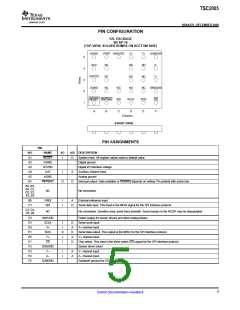
TSC2005
www.ti.com
SBAS379–DECEMBER 2006
This integrated circuit can be damaged by ESD. Texas Instruments recommends that all integrated circuits be handled with
appropriate precautions. Failure to observe proper handling and installation procedures can cause damage.
ESD damage can range from subtle performance degradation to complete device failure. Precision integrated circuits may be
more susceptible to damage because very small parametric changes could cause the device not to meet its published
specifications.
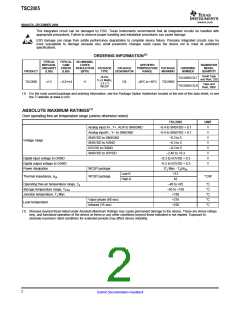
ORDERING INFORMATION(1)
TYPICAL
INTEGRAL
LINEARITY
(LSB)
TYPICAL
GAIN
ERROR
(LSB)
NO MISSING
CODES
RESOLUTION PACKAGE
SPECIFIED
TEMPERATURE PACKAGE
TRANSPORT
MEDIA,
QUANTITY
PACKAGE
DESIGNATOR
ORDERING
NUMBER
PRODUCT
(BITS)
TYPE
RANGE
MARKING
Small Tape
and Reel, 250
18-Pin,
5 x 6 Matrix,
2.5 x 3
TSC2005IYZLT
TSC2005IYZLR
TSC2005
±1.5
– 0.2/+4.4
11
YZL
–40°C to +85°C
TSC2005I
Tape and
Reel, 3000
WCSP
(1) For the most current package and ordering information, see the Package Option Addendum located at the end of this data sheet, or see
the TI website at www.ti.com.
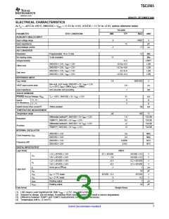
ABSOLUTE MAXIMUM RATINGS(1)
Over operating free-air temperature range (unless otherwise noted)
TSC2005
–0.4 to SNSVDD + 0.1
–0.4 to SNSVDD + 0.1
–0.3 to 5
UNIT
V
Analog input X+, Y+, AUX to SNSGND
Analog inputX–, Y– to SNSGND
SNSVDD to SNSGND
V
V
Voltage range
SNSVDD to AGND
–0.3 to 5
V
I/OVDD to DGND
–0.3 to 5
V
SNSVDD to I/OVDD
–2.40 to +0.3
–0.3 to I/OVDD + 0.3
–0.3 to I/OVDD + 0.3
(TJ Max - TA)/θJA
113
V
Digital input voltage to DGND
Digital output voltage to DGND
Power dissipation
V
V
WCSP package
Low-K
WCSP package
Thermal impedance, θJA
°C/W
High-K
62
Operating free-air temperature range, TA
Storage temperature range, TSTG
Junction temperature, TJ Max
–40 to +85
°C
°C
°C
°C
°C
–65 to +150
+150
Vapor phase (60 sec)
Infrared (15 sec)
+215
Lead temperature
+220
(1) Stresses beyond those listed under Absolute Maximum Ratings may cause permanent damage to the device. These are stress ratings
only, and functional operation of the device at these or any other conditions beyond those indicated is not implied. Exposure to
absolute-maximum rated conditions for extended periods may affect device reliability.
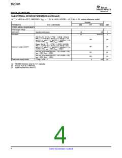
2
Submit Documentation Feedback

 BB [ BURR-BROWN CORPORATION ]