ꢀ ꢁꢂ ꢃ ꢄꢅ ꢆ
www.ti.com
SLES100 − DECEMBER 2003
APPLICATION INFORMATION
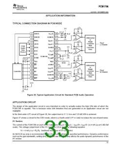
TYPICAL CONNECTION DIAGRAM IN PCM MODE
C
f
5 V
R
R
f
0.1 µF
ZEROL
ZEROR
MSEL
LRCK
DATA
BCK
V
2L
1
2
28
27
26
25
24
23
22
21
20
19
18
17
16
15
10 µF
CC
−
+
AGND3L
Differential
to
I L−
OUT
3
C
f
Single
Converter
With
Low-Pass
Filter
V
OUT
L-Channel
I
L+
4
OUT
f
PCM
Audio
Data
5 V
AGND2
5
−
+
V
1
CC
6
Source
10 µF
SCK
V L
COM
7
+
C
f
PCM1796
DGND
V
COM
R
8
R
R
0.1 µF
47 µF
10 kΩ
f
V
DD
I
REF
9
−
+
MS
AGND1
10
11
12
13
14
Differential
to
Single
Converter
With
Low-Pass
Filter
MDI
MC
I
R−
R+
C
OUT
f
V
OUT
R-Channel
Controller
I
OUT
f
0.1 µF
5 V
AGND3R
MDO
RST
−
+
V
CC
2R
10 µF
3.3 V
+
10 µF
Figure 35. Typical Application Circuit for Standard PCM Audio Operation
APPLICATION CIRCUIT
The design of the application circuit is very important in order to actually realize the high S/N ratio of which the
PCM1796 is capable. This is because noise and distortion that are generated in an application circuit are not
negligible.
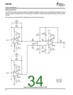
In the third-order LPF circuit of Figure 36, the output level is 2.1 V rms and 123 dB S/N is achieved.
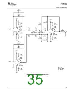
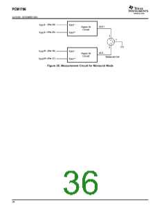
Figure 37 shows a circuit for the DSD mode, which is a fourth-order LPF in order to reduce the out-of-band noise.
I/V Section
The current of the PCM1796 on each of the output pins (I
L+, I
L–, I
R+, I
R–) is 4 mA p-p at 0 dB (full
OUT
OUT
OUT
OUT
scale). The voltage output level of the I/V converter (Vi) is given by following equation:
Vi = 4 mA p−p × R (R : feedback resistance of I/V converter)
f
f
An NE5534 op amp is recommended for the I/V circuit to obtain the specified performance. Dynamic performance
such as the gain bandwidth, settling time, and slew rate of the op amp affects the audio dynamic performance of the
I/V section.
33

 BB [ BURR-BROWN CORPORATION ]