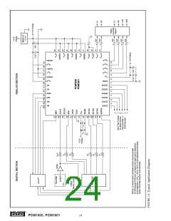
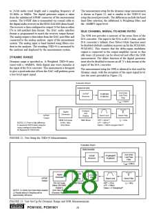
Separate power supplies are recommended for the digital
and analog sections of the board. This prevents the switching
noise present on the digital supply from contaminating the
analog power supply and degrading the dynamic perfor-
mance of the D/A converters. In cases where a common +5V
supply must be used for the analog and digital sections, an
inductance (RF choke, ferrite bead) should be placed be-
tween the analog and digital +5V supply connections to
avoid coupling of the digital switching noise into the analog
circuitry. Figure 18 shows the recommended approach for
single-supply applications.
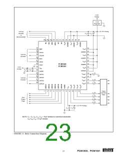
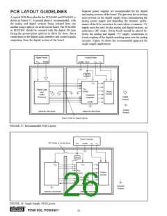
PCB LAYOUT GUIDELINES
A typical PCB floor plan for the PCM1600 and PCM1601 is
shown in Figure 17. A ground plane is recommended, with
the analog and digital sections being isolated from one
another using a split or cut in the circuit board. The PCM1600
or PCM1601 should be oriented with the digital I/O pins
facing the ground plane split/cut to allow for short, direct
connections to the digital audio interface and control signals
originating from the digital section of the board.
Digital Power
Analog Power
+VD
DGND
AGND +5VA
+VS –VS
REG
VCC
VDD
DGND
Digital Logic
and
Audio
Processor
Output
Circuits
PCM1600
PCM1601
Digital
Ground
AGND
Analog
Ground
DIGITAL SECTION
ANALOG SECTION
Return Path for Digital Signals
FIGURE 17. Recommended PCB Layout.
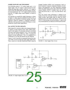
Power Supplies
RF Choke or Ferrite Bead
+5V
AGND +VS –VS
REG
VCC
VDD
VDD
DGND
Output
Circuits
PCM1600
PCM1601
AGND
Common
Ground
DIGITAL SECTION
ANALOG SECTION
FIGURE 18. Single-Supply PCB Layout.
®
26
PCM1600, PCM1601

 BB [ BURR-BROWN CORPORATION ]