ZERO FLAG AND INFINITE ZERO DETECT MUTE
FUNCTIONS
ANALOG OUTPUTS
The PCM1600 includes six independent output channels,
VOUT1 through VOUT6. These are unbalanced outputs, each
capable of driving 3.1Vp-p typical into a 5kΩ AC load with
VCC = +5V. The internal output amplifiers for VOUT1 through
VOUT6 are DC biased to the common-mode (or bipolar zero)
voltage, equal to VCC/2.
The PCM1600 includes circuitry for detecting an all ‘0’ data
condition for the data input pins, DATA1 through DATA3.
This includes two independent functions: Zero Output Flags
and Zero Detect Mute.
Although the flag and mute functions are independent of one
another, the zero detection mechanism is common to both
functions.
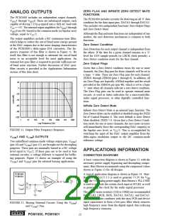
The output amplifiers include a RC continuous-time filter,
which helps to reduce the out-of-band noise energy present
at the DAC outputs due to the noise shaping characteristics
of the PCM1600’s delta-sigma D/A converters. The fre-
quency response of this filter is shown in Figure 11. By
itself, this filter is not enough to attenuate the out-of-band
noise to an acceptable level for most applications. An
external low-pass filter is required to provide sufficient out-
of-band noise rejection. Further discussion of DAC post-
filter circuits is provided in the Applications Information
section of this data sheet.
Zero Detect Condition
Zero Detection for each output channel is independent from
the others. If the data for a given channel remains at a ‘0’
level for 1024 sample periods (or LRCK clock periods), a
Zero Detect condition exists for the that channel.
Zero Output Flags
Given that a Zero Detect condition exists for one or more
channels, the Zero flag pins for those channels will be set to
a logic ‘1’state. There are Zero Flag pins for each channel,
ZERO1 through ZERO6 (pins 1 through 6). In addition, all
six Zero Flags are logically ANDed together and the result
provided at the ZEROA pin (pin 48), which is set to a logic
‘1’ state when all channels indicate a zero detect condition.
The Zero Flag pins can be used to operate external mute
circuits, or used as status indicators for a microcontroller,
audio signal processor, or other digitally controlled func-
tions.
20
0
–20
–40
–60
–80
–100
Infinite Zero Detect Mute
Infinite Zero Detect Mute is an internal logic function. The
Zero Detect Mute can be enabled or disabled using the INZD
bit of Control Register 8. The reset default is Zero Detect
Mute disabled, INZD = 0. Given that a Zero Detect Condi-
tion exists for one or more channels, the zero mute circuitry
will immediately force the corresponding DAC output(s) to
the bipolar zero level, or VCC/2. This is accomplished by
switching the input of the DAC output amplifier from the
delta-sigma modulator output to the DC common-mode
reference voltage.
1
10
100
1k
10k
100k
1M
10M
Log Frequency (Hz)
FIGURE 11. Output Filter Frequency Response.
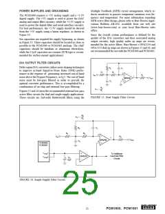
VCOM1 AND VCOM2 OUTPUTS
Two unbuffered common-mode voltage output pins, VCOM1
(pin 16) and VCOM2 (pin 15), are brought out for decoupling
purposes. These pins are nominally biased to a DC voltage
level equal to VCC/2. If these pins are to be used to bias
external circuitry, a voltage follower is required for buffer-
ing purposes. Figure 12 shows an example of using the
VCOM1 and VCOM2 pins for external biasing applications.
APPLICATIONS INFORMATION
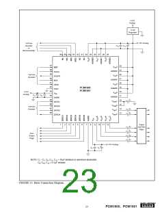
CONNECTION DIAGRAMS
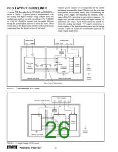
A basic connection diagram is shown in Figure 13, with the
necessary power supply bypassing and decoupling compo-
nents. Burr-Brown recommends using the component values
shown in Figure 13 for all designs.
PCM1600
PCM1601
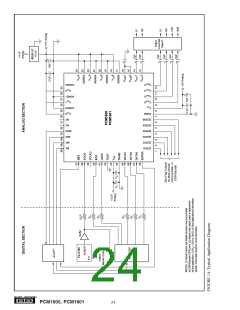
A typical application diagram is shown in Figure 14. Burr-
Brown’s REG1117-3.3 is used to generate +3.3V for VDD
from the +5V analog power supply. Burr-Brown’s PLL1700E
is used to generate the system clock input at SCLKI, as well
as generating the clock for the audio signal processor.
4
VCC
2
1
VBIAS
≈
OPA337
3
16
15
VCOM
1
V
COM2
+
10µF
The use of series resistors (22Ω to 100Ω) are recommended
for SCLKI, LRCK, BCK, DATA1, DATA2, and DATA3.
The series resistor combines with the stray PCB and device
input capacitance to form a low-pass filter which removes
high frequency noise from the digital signal, thus reducing
high frequency emission.
FIGURE 12. Biasing External Circuits Using the VCOM
1
and VCOM2 Pins.
®
22
PCM1600, PCM1601

 BB [ BURR-BROWN CORPORATION ]