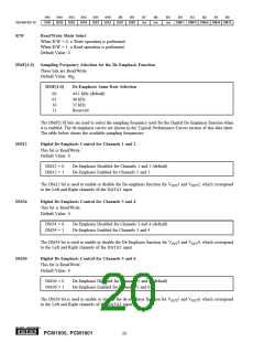
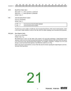
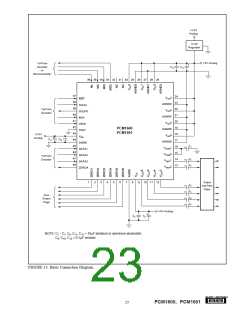
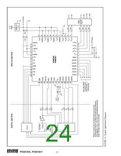
POWER SUPPLIES AND GROUNDING
Multiple Feedback (MFB) circuit arrangement, which re-
duces sensitivity to passive component variations over fre-
quency and temperature. For more information regarding
MFB active filter design, please refer to Burr-Brown Appli-
cations Bulletin AB-034, available from our web site
(www.burr-brown.com) or your local Burr-Brown sales
office.
The PCM1600 requires a +5V analog supply and a +3.3V
digital supply. The +5V supply is used to power the DAC
analog and output filter circuitry, while the +3.3V supply is
used to power the digital filter and serial interface circuitry.
For best performance, the +3.3V supply should be derived
from the +5V supply using a linear regulator, as shown in
Figure 14.
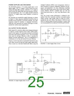
Since the overall system performance is defined by the
quality of the D/A converters and their associated analog
output circuitry, high quality audio op amps are recom-
mended for the active filters. Burr-Brown’s OPA2134 and
OPA2353 dual op amps are shown in Figures 15 and 16, and
are recommended for use with the PCM1600 and PCM1601.
Six capacitors are required for supply bypassing, as shown
in Figure 13. These capacitors should be located as close as
possible to the PCM1600 or PCM1601 package. The 10µF
capacitors should be tantalum or aluminum electrolytic,
while the 0.1µF capacitors are ceramic (X7R type is recom-
mended for surface-mount applications).
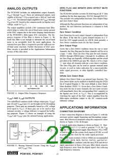
D/A OUTPUT FILTER CIRCUITS
Delta-sigma D/A converters utilize noise shaping techniques
to improve in-band Signal-to-Noise Ratio (SNR) perfor-
mance at the expense of generating increased out-of-band
noise above the Nyquist Frequency, or fS/2. The out-of-band
noise must be low-pass filtered in order to provide the
optimal converter performance. This is accomplished by a
combination of on-chip and external low-pass filtering.
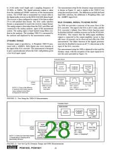
R2
C1
2
R1
R3
VIN
R4
1
VOUT
OPA2134
3
C2
R2
R1
A
V ≈ –
Figures 15 and 16 show the recommended external low-pass
active filter circuits for dual and single-supply applications.
These circuits are 2nd-order Butterworth filters using the
FIGURE 15. Dual Supply Filter Circuit.
R2
A
V ≈ –
R1
R2
C1
R1
R3
2
VIN
R4
1
VOUT
OPA2134
C2
3
PCM1600
PCM1601
VCOM
VCOM
1
To Additional
Low-Pass Filter
Circuits
OPA337
2
C2
10µF
+
FIGURE 16. Single-Supply Filter Circuit.
®
25
PCM1600, PCM1601

 BB [ BURR-BROWN CORPORATION ]