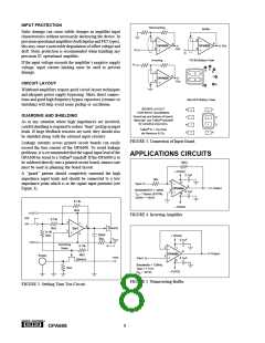
1MΩ
+15V
7
10kΩ
C1
20pF
2
3
Output
Voltage
EO
Current
Input
i
2
3
Load
R1
6
6
OPA606
OPA606
100Ω
Input
4
EO = |i| R = 1V/µA
Optimize response for particular
load condition with C1 and R1.
1MΩ
–15V
i
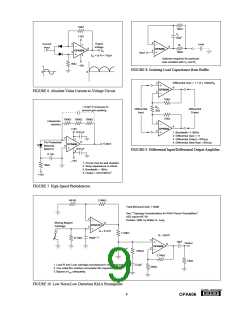
FIGURE 8. Isolating Load Capacitance from Buffer.
0
0
Differential Gain = 1 + (2 x 10kΩ)/RG
3
2
6
OPA606
FIGURE 6. Absolute Value Current-to-Voltage Circuit.
10kΩ
≈ 0.2pF if necessary to
prevent gain peaking
RG
2kΩ
Differential
Input
Differential
Output
10kΩ
150kΩ 150kΩ 150kΩ
3 Metal-film
resistors
2
6
OPA606
+15V
3
0.01µF
1. Bandwidth ≈1.2MHz
2. Differential Gain = 11
3. Differential Output ≈ 50Vp-p
4. Differential Slew Rate ≈ 65V/µs
2
7
OPA606
6
Pin Photodiode
Motorola
Output
3
0.01µF
MRD721
FIGURE 9. Differential Input/Differential Output Amplifier.
4
0.1µF
–15V
1. Circuit must be well shielded.
2. Stray capacitance is critical.
3. Bandwidth ≈ 1MHz
10kΩ
4. Output ≈ 22V/mW/cm2
+15V
FIGURE 7. High-Speed Photodetector.
49.9Ω
2.49kΩ
Total Mid-band Gain = 40dB
See: "Topology Considerations for RIAA Phono Preamplifiers".
AES reprint #1719.
October 1980, by Walter G. Jung
2
Moving Magnet
Cartridge
6
OPA37EJ
3
G ≈ 51V/V
7.32kΩ
G ≈ 20V/V
47.5kΩ
150pF (1)
3
2
10µF
Output
6
OPA606
0.1µF
1.05kΩ
3.74kΩ
10kΩ
0.3µF
1. Load R and C per cartridge manufacturer's recommendations.
2. Use metal film resistors and plastic film capacitors.
3. Bypass ±VCC adequately.
200Ω
FIGURE 10. Low Noise/Low Distortion RIAA Preamplifier.
9
®
OPA606

 BB [ BURR-BROWN CORPORATION ]