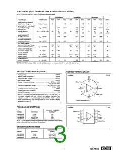
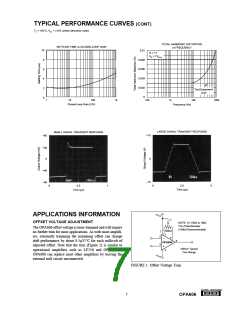
INPUT PROTECTION
Noninverting
2
Buffer
Static damage can cause subtle changes in amplifier input
characteristics without necessarily destroying the device. In
precision operational amplifiers (both bipolar and FET types),
this may cause a noticeable degradation of offset voltage and
drift. Static protection is recommended when handling any
precision IC operational amplifier.
2
3
6
6
Out
OPA606
OPA606
3
Out
In
In
Inverting
TO-99 Bottom View
If the input voltage exceeds the amplifier’s negative supply
voltage, input current limiting must be used to prevent
damage.
In
5
4
6
7
2
3
2
6
OPA606
3
Out
CIRCUIT LAYOUT
8
1
Wideband amplifiers require good circuit layout techniques
and adequate power supply bypassing. Short, direct connec-
tions and good high frequency bypass capacitors (ceramic or
tantalum) will help avoid noise pickup or oscillation.
Mini-DIP Bottom View
BOARD LAYOUT
1
8
FOR INPUT GUARDING
GUARDING AND SHIELDING
Guard top and bottom of board.
Alternate: use Teflon® standoff
for sensitive input pins.
2
3
7
6
5
As in any situation where high impedances are involved,
careful shielding is required to reduce “hum” pickup in input
leads. If large feedback resistors are used, they should also
be shielded along with the external input circuitry.
Teflon® E. I. Du Pont
de Nemours & Co.
4
FIGURE 3. Connection of Input Guard.
Leakage currents across printed circuit boards can easily
exceed the bias current of the OPA606. To avoid leakage
problems, it is recommended that the signal input lead of the
OPA606 be wired to a Teflon® standoff. If the OPA606 is to
be soldered directly into a printed circuit board, utmost care
must be used in planning the board layout.
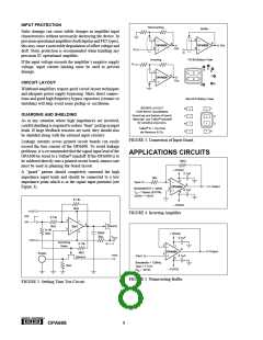
APPLICATIONS CIRCUITS
10kΩ
+15VDC
0.1µF
A “guard” pattern should completely surround the high
impedance input leads and should be connected to a low
impedance point which is at the signal input potential (see
Figure 3).
1kΩ
2
7
Input
6
Output
OPA606
BANDWIDTH > 1MHz
S ≈ 1.8µsec (0.01%)
GAIN = –10V/V
3
0.1µF
4
T
0.1%
–15VDC
2kΩ
+15V
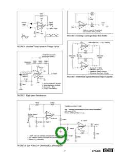
FIGURE 4. Inverting Amplifier.
+5V
0.1%
2
7
4
–5V
6
2N4416
2kΩ
0.1%
5kΩ
DUT
3
100pF
3k
+15VDC
Ω
VOUT
0.1µF
–15V
Summing
Node
0.1%
G = –1
2
3
7
6
Output
OPA606
5kΩ
Scope
+15V
0.1µF
Input
2N4416
4
Bandwidth > 12MHz
Gain = +1V/V
R
2kΩ
IN ≈ 1013Ω
–15VDC
FIGURE 5. Noninverting Buffer.
FIGURE 2. Settling Time Test Circuit.
®
8
OPA606

 BB [ BURR-BROWN CORPORATION ]