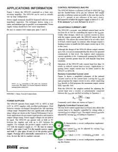
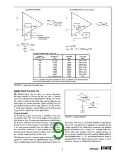
(a) RESISTOR METHOD
(b) DAC METHOD (Current or Voltage)
Max IO = ILIM
Max IO = ILIM
(4.75) (15800)
±ILIM
=
±ILIM =15800 ISET
7500Ω + RCL
7500Ω
7500Ω
4.75V
4.75V
ISET
8
8
D/A
Ref
Ref
RCL
0.01µF
(optional, for noisy
environments)
6
6
15800 (4.75V)
ILIM
RCL
=
=
– 7500Ω
– 7.5kΩ
ISET = ILIM/15800
SET = (Ref) + 4.75V – (7500Ω) (ILIM)/15800
75kΩ
V
ILIM
OPA549 CURRENT LIMIT: 0A to 10A
DESIRED
CURRENT LIMIT
RESISTOR(1)
(RCL
CURRENT
(ISET
VOLTAGE
(VSET
)
)
)
0A(2)
2.5A
3A
4A
5A
6A
7A
8A
9A
I
LIM Open
22.6kΩ
17.4kΩ
11.3kΩ
7.5kΩ
4.99kΩ
3.24kΩ
1.87kΩ
845Ω
0µA
(Ref) + 4.75V
(Ref) + 3.56V
(Ref) + 3.33V
(Ref) + 2.85V
(Ref) + 2.38V
(Ref) + 1.90V
(Ref) + 1.43V
(Ref) + 0.95V
(Ref) + 0.48V
(Ref)
158µA
190µA
253µA
316µA
380µA
443µA
506µA
570µA
633µA
10A
ILIM Connected to Ref
NOTES: (1) Resistors are nearest standard 1% values. (2) Offset in the current limit circuitry
may introduce approximately ±0.25A variation at low current limit values.
FIGURE 2. Adjustable Current Limit.
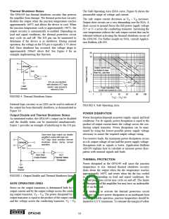
ENABLE/STATUS (E/S) PIN
The Enable/Status Pin provides two unique functions:
1) output disable by forcing the pin low and 2) thermal
shutdown indication by monitoring the voltage level at the
pin. Either or both of these functions can be utilized in an
application. For normal operation (output enabled), the E/S
pin can be left open or driven high (at least 2.4V above Ref).
A small value capacitor connected between the E/S pin and
CREF may be required for noisy applications.
OPA549
E/S
Ref
CMOS or TTL
Logic
Ground
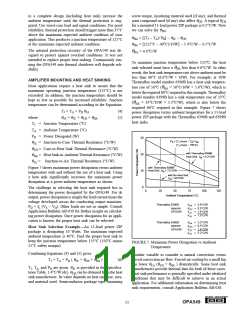
Output Disable
To disable the output, the E/S pin is pulled to a logic low
(no greater than 0.8V above Ref). Typically the output is
shut down in 1µs. To return the output to an enabled state,
the E/S pin should be disconnected (open) or pulled to at
least 2.4V above Ref. It should be noted that driving the E/
S pin high (output enabled) does not defeat internal ther-
mal shutdown; however, it does prevent the user from
monitoring the thermal shutdown status. See Figure 3 for
an example implementing this function.
FIGURE 3. Output Disable.
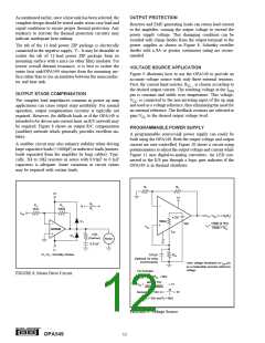
shows two OPA549s in a switched amplifier configuration.
The on/off state of the two amplifiers is controlled by the
voltage on the E/S pin. Under these conditions, the disabled
device will behave like a 750pF load. Slewing faster than
3V/µs will cause leakage current to rapidly increase in
devices that are disabled, and will contribute additional load.
At high temperature (125°C), the slewing threshold drops to
approximately 2V/µs. Input signals must be limited to avoid
excessive slewing in multiplexed applications.
This function not only conserves power during idle periods
(quiescent current drops to approximately 6mA) but also
allows multiplexing in multi-channel applications. Figure 12
®
9
OPA549

 BB [ BURR-BROWN CORPORATION ]