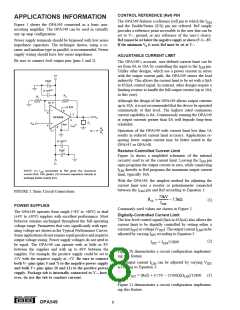
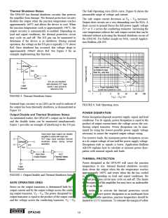
Thermal Shutdown Status
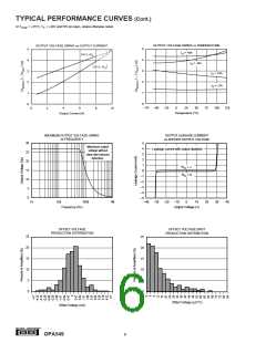
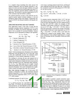
The Safe Operating Area (SOA curve, Figure 6) shows the
permissible range of voltage and current.
The OPA549 has thermal shutdown circuitry that protects
the amplifier from damage. The thermal protection circuitry
disables the output when the junction temperature reaches
approximately 160°C and allows the device to cool. When
the junction temperature cools to approximately 140°C, the
output circuitry is automatically re-enabled. Depending on
load and signal conditions, the thermal protection circuit
may cycle on and off. The E/S pin can be monitored to
determine if the device is in shutdown. During normal
operation, the voltage on the E/S pin is typically 3.5V above
Ref. Once shutdown has occurred, this voltage drops to
approximately 200mV above Ref. See Figure 4 for an
example implementing this function.
The safe output current decreases as VS – VO increases.
Output short circuits are a very demanding case for SOA. A
short circuit to ground forces the full power supply voltage
(V+ or V–) across the conducting transistor. Increasing the
case temperature reduces the safe output current that can be
tolerated without activating the thermal shutdown circuit of
the OPA549. For further insight on SOA, consult Applica-
tion Bulletin AB-039.
20
10
PD = 90W
TC = 25°C
PD = 47W
OPA549
Output current can
be limited to less
than 8A—see text.
E/S
Ref
PD = 18W
1
HCT
E/S pin can interface
TC = 85°C
with standard HCT logic
inputs. Logic ground is
Logic
Ground
TC = 125°C
Pulse Operation Only
(Limit rms current to ≤ 8A)
referred to Ref.
0.1
1
2
5
10
20
50
100
FIGURE 4. Thermal Shutdown Status.
VS
– VO (V)
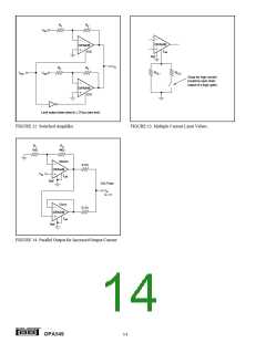
External logic circuitry or an LED can be used to indicate if
the output has been thermally shutdown, as demonstrated in
Figure 10.
FIGURE 6. Safe Operating Area.
POWER DISSIPATION
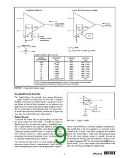
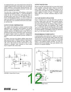
Output Disable and Thermal Shutdown Status
As mentioned earlier, the OPA549’s output can be disabled
and the disable status can be monitored simultaneously.
Figure 5 provides an example of interfacing to the E/S pin.
Power dissipation depends on power supply, signal, and load
conditions. For dc signals, power dissipation is equal to the
product of output current times the voltage across the con-
ducting output transistor. Power dissipation can be mini-
mized by using the lowest possible power supply voltage
necessary to assure the required output voltage swing.
Open-drain logic output can disable
amplifier's output with logic low.
For resistive loads, the maximum power dissipation occurs
at a dc output voltage of one-half the power supply voltage.
Dissipation with ac signals is lower. Application Bulletin
AB-039 explains how to calculate or measure power dissi-
pation with unusual signals and loads.
HCT logic input monitors thermal
shutdown status during normal
operation.
OPA549
E/S
Ref
Open Drain
(Output Disable)
HCT
(Thermal Status
Shutdown)
THERMAL PROTECTION
Power dissipated in the OPA549 will cause the junction
temperature to rise. Internal thermal shutdown circuitry
shuts down the output when the die temperature reaches
approximately 160°C and resets when the die has cooled
to 140°C. Depending on load and signal conditions, the
thermal protection circuit may cycle on and off. This limits
the dissipation of the amplifier but may have an undesirable
effect on the load.
Logic
Ground
FIGURE 5. Output Disable and Thermal Shutdown Status.
SAFE OPERATING AREA
Stress on the output transistors is determined both by the
output current and by the output voltage across the conduct-
ing output transistor, VS – VO. The power dissipated by the
output transistor is equal to the product of the output current
and the voltage across the conducting transistor, VS – VO.
Any tendency to activate the thermal protection circuit
indicates excessive power dissipation or an inadequate heat
sink. For reliable operation, junction temperature should be
limited to 125°C maximum. To estimate the margin of safety
®
OPA549
10

 BB [ BURR-BROWN CORPORATION ]