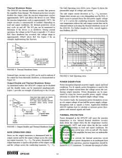
As mentioned earlier, once a heat sink has been selected, the
complete design should be tested under worst-case load and
signal conditions to ensure proper thermal protection. Any
tendency to activate the thermal protection circuitry may
indicate inadequate heat sinking.
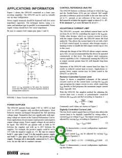
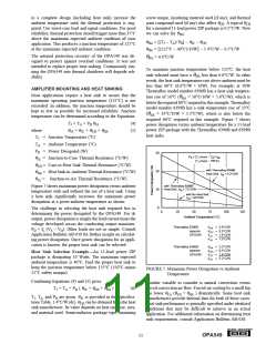
OUTPUT PROTECTION
Reactive and EMF-generating loads can return load current
to the amplifier, causing the output voltage to exceed the
power supply voltage. This damaging condition can be
avoided with clamp diodes from the output terminal to the
power supplies as shown in Figure 8. Schottky rectifier
diodes with a 8A or greater continuous rating are recom-
mended.
The tab of the 11-lead power ZIP package is electrically
connected to the negative supply, V–. It may be desirable to
isolate the tab of 11-lead power ZIP package from its
mounting surface with a mica (or other film) insulator. For
lowest overall thermal resistance, it is best to isolate the
entire heat sink/OPA549 structure from the mounting sur-
face rather than to use an insulator between the semiconduc-
tor and heat sink.
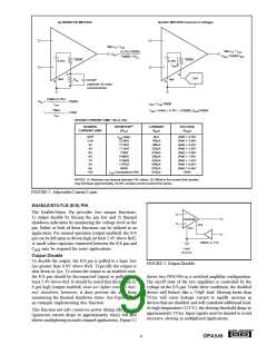
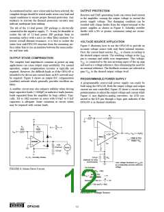
VOLTAGE SOURCE APPLICATION
Figure 9 illustrates how to use the OPA549 to provide an
accurate voltage source with only three external resistors.
First, the current limit resistor, RCL , is chosen according to
the desired output current. The resulting voltage at the ILIM
pin is constant and stable over temperature. This voltage,
VCL, is connected to the non-inverting input of the op amp
and used as a voltage reference, thus eliminating the need for
an external reference. The feedback resistors are selected to
gain VCL to the desired output voltage level.
OUTPUT STAGE COMPENSATION
The complex load impedances common in power op amp
applications can cause output stage instability. For normal
operation, output compensation circuitry is typically not
required. However, for difficult loads or if the OPA549 is
intended to be driven into current limit, an R/C network may
be required. Figure 8 shows an output R/C compensation
(snubber) network which generally provides excellent sta-
bility.
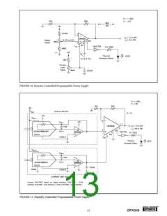
PROGRAMMABLE POWER SUPPLY
A programmable source/sink power supply can easily be
built using the OPA549. Both the output voltage and output
current are user-controlled. Figure 10 shows a circuit using
potentiometers to adjust the output voltage and current while
Figure 11 uses digital-to-analog converters. An LED con-
nected to the E/S pin through a logic gate indicates if the
OPA549 is in thermal shutdown.
A snubber circuit may also enhance stability when driving
large capacitive loads (>1000pF) or inductive loads (motors,
loads separated from the amplifier by long cables). Typi-
cally, 3Ω to 10Ω resistors in series with 0.01µF to 0.1µF
capacitors is adequate. Some variations in circuit values
may be required with certain loads.
R1
R2
V+
V+
R2
R1
5kΩ
R2
20kΩ
G = –
= –4
R1
VIN
VO = VCL (1 + R2/R1)
15800 (4.75V)
4.75V
7500Ω
D1
Ref
IO
=
VCL
7500Ω + RCL
OPA549
ILIM
10Ω
(Carbon)
D2
Motor
V–
0.01µF
V–
D1, D2 : Schottky Diodes
0.01µF
RCL
(Optional, for noisy
environments)
Uses voltage developed at ILIM pin
as a moderately accurate reference
voltage.
For Example:
FIGURE 8. Motor Drive Circuit.
If ILIM = 7.9A, RCL = 2kΩ
2kΩ • 4.75V
VCL
=
= 1V
(2kΩ + 7500Ω)
10
1
Desired VO = 10V,G =
= 10
R1 = 1kΩ and R2 = 9kΩ
FIGURE 9. Voltage Source.
®
OPA549
12

 BB [ BURR-BROWN CORPORATION ]