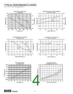
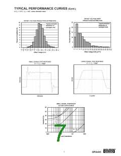
HEAT SINKING
SAFE OPERATING AREA
Power dissipated in the OPA445 will cause the junction
temperature to rise. For reliable operation junction tempera-
ture should be limited to 125°C, maximum (150°C for
TO-99 package). Some applications will require a heat sink
to assure that the maximum operating junction temperature
is not exceeded. In addition, the junction temperature should
be kept as low as possible for increased reliability. Junction
temperature can be determined according to the following
equation:
100
10
1
TA = 25°C
TA = 85°C
TA = 120°C
TA + (|VS| – |VO|) IOθJA ≤ TJ (max)
JA = 150°C/W
TJ (max) = 125°C
TJ = TA + PD θJA
θ
0.1
Package thermal resistance, θJA, is affected by mounting
techniques and environments. Poor air circulation and use of
sockets can significantly increase thermal resistance. Best
thermal performance is achieved by soldering the op amp into
a circuit board with wide printed circuit traces to allow greater
conduction through the op amp leads. Simple clip-on heat
sinks (such as Thermalloy 2257) can reduce the thermal
resistance of the TO-99 metal package by as much as 50°C/W.
For additional information on determining heat sink require-
ments, consult Applications Bulletin AB-038.
1
2
5
10
|VS| – |VO| (V)
20
50
100
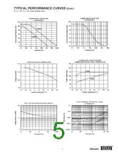
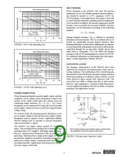
FIGURE 4. SO-8 Safe Operating Area.
SAFE OPERATING AREA
100
TA = 25°C
10
TA = 125°C
CAPACITIVE LOADS
TA = 85°C
The dynamic characteristics of the OPA445 have been
optimized for commonly encountered gains, loads, and op-
erating conditions. The combination of low closed-loop gain
and capacitive load will decrease the phase margin and may
lead to gain peaking or oscillations. Figure 6 shows a circuit
which preserves phase margin with capacitive load. The
circuit does not suffer a voltage drop due to load current,
however, input impedance is reduced at high frequencies.
Consult Application Bulletin AB-028 for details of analysis
techniques and application circuits.
1
TA + (|VS| – |VO|) IOθJA ≤ TJ (max)
θ
JA = 200°C/W (No Heat Sink
*)
TJ (max) = 150°C
*
Simple clip-on heatsinks can
reduce θ by as much as 50°C/W.
0.1
1
2
5
10
20
50
100
|VS| – |VO| (V)
FIGURE 5. TO-99 Safe Operating Area.
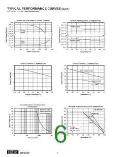
POWER DISSIPATION
R1
R2
Power dissipation depends on power supply, signal, and load
conditions. For dc signals, power dissipation is equal to the
product of the output current times the voltage across the
conducting output transistor, PD = IL (VS – VO). Power
dissipation can be minimized by using the lowest possible
power supply voltage necessary to assure the required output
voltage swing.
2kΩ
2kΩ
R2
R1
RC
20Ω
G = 1 +
CC
0.22µF
OPA445
VO
VIN
For resistive loads, the maximum power dissipation occurs
at a dc output voltage of one-half the power supply voltage.
Dissipation with ac signals is lower. Application Bulletin
AB-039 explains how to calculate or measure dissipation
with unusual loads or signals.
CL
5000pF
R2
RC
CC
=
=
2CL X 1010 – (1 + R2/R1)
CL X 103
RC
The OPA445 can supply output currents of 15mA and
larger. This would present no problem for a standard op amp
operating from ±15V supplies. With high supply voltages,
however, internal power dissipation of the op amp can be
quite large. Operation from a single power supply (or unbal-
anced power supplies) can produce even larger power dissi-
pation since a large voltage is impressed across the conduct-
ing output transistor. Applications with large power dissipa-
tion may require a heat sink.
NOTE: Design equations and component values are approximate.
User adjustment is required for optimum performance.
FIGURE 6. Driving Large Capacitive Loads.
®
9
OPA445

 BB [ BURR-BROWN CORPORATION ]