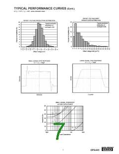
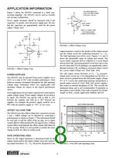
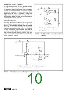
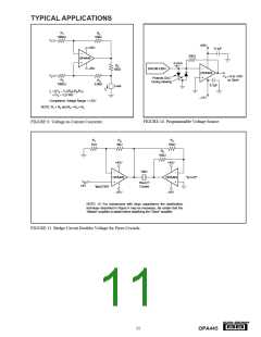
APPLICATION INFORMATION
Figure 1 shows the OPA445 connected as a basic non-
inverting amplifier. The OPA445 can be used in virtually
any op amp configuration.
Use offset adjust pins
only to null offset voltage
of op amp—see text.
V+
7
2
3
6
Power supply terminals should be bypassed with 0.1µF
capacitors, or greater, near the power supply pins. Be sure
that the capacitors are appropriately rated for the power
supply voltage used.
OPA445
1
10mV Typical
Trim Range
5
4
(1)
NOTE: (1) 10kΩ to 1MΩ
Trim Potentiometer
V–
(100kΩ recommended).
V+
0.1µF
R2
G = 1+
R1
R1
R2
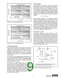
FIGURE 2. Offset Voltage Trim.
VO
OPA445
output transistor is equal to the product of the output current
and the voltage across the conducting transistor, VS – VO.
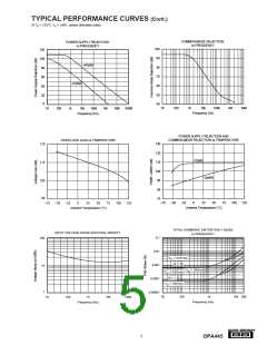
The Safe Operating Area (SOA curve, Figures 3, 4, and 5)
shows the permissible range of voltage and current. The
curves shown represent devices soldered to a circuit board
with no heat sink. Increasing printed circuit trace area or the
use of a heat sink (TO-99 package) can significantly reduce
thermal resistance (θ), resulting in increased output current
for a given output voltage (see “Heat Sink” text).
VIN
ZL
0.1µF
V–
FIGURE 1. Offset Voltage Trim.
The safe output current decreases as VS – VO increases.
Output short-circuits are a very demanding case for SOA. A
short-circuit to ground forces the full power supply voltage
(V+ or V–) across the conducting transistor and produces a
typical output current of 25mA. With ±40V power supplies,
this creates an internal dissipation of 1W. This exceeds the
maximum rating and is not recommended. If operation in
this region is unavoidable, a heat sink is required. For further
insight on SOA, consult Application Bulletin AB-039.
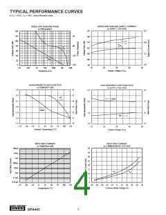
POWER SUPPLIES
The OPA445 may be operated from power supplies up to
±45V or a total of 90V with excellent performance. Most
behavior remains unchanged throughout the full operating
voltage range. Parameters which vary significantly with
operating voltage are shown in the typical performance
curves.
Some applications do not require equal positive and negative
output voltage swing. Power supply voltages do not need to
be equal. The OPA445 can operate with as little as 20V
between the supplies and with up to 90V between the
supplies. For example, the positive supply could be set to
80V with the negative supply at –10V, or vice-versa.
SAFE OPERATING AREA
100
OFFSET VOLTAGE TRIM
TA = 25°C
TheOPA445providesoffsetvoltagetrimconnectionsonpins
1 and 5. Offset voltage can be adjusted by connecting a
potentiometer as shown in Figure 2. This adjustment should
be used only to null the offset of the op amp, not to adjust
system offset or offset produced by the signal source. Nulling
system offset could degrade the offset voltage drift behavior
of the op amp. While it is not possible to predict the exact
change in drift, the effect is usually small.
10
TA = 85°C
TA = 120°C
1
TA + (|VS| – |VO|) IOθJA ≤ TJ (max)
θ
JA = 100°C/W
TJ (max) = 125°C
0.1
1
2
5
10
20
50
100
|VS| – |VO| (V)
SAFE OPERATING AREA
Stress on the output transistors is determined both by the
output current and by the output voltage across the conduct-
ing output transistors, VS – VO. The power dissipated by the
FIGURE 3. 8-Pin DIP Safe Operating Area.
®
8
OPA445

 BB [ BURR-BROWN CORPORATION ]