THE GAIN EQUATION
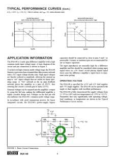
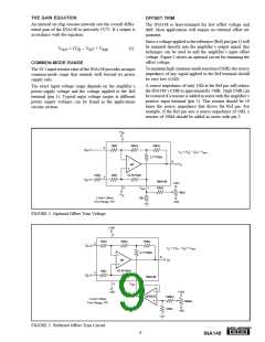
OFFSET TRIM
An internal on-chip resistor network sets the overall differ-
ential gain of the INA148 to precisely 1V/V. It’s output is
accordance with the equation:
The INA148 is laser-trimmed for low offset voltage and
drift. Most applications will require no external offset ad-
justment.
Since a voltage applied to the reference (Ref) pin (pin 1) will
be summed directly into the amplifier’s output signal, this
technique can be used to null the amplifier’s input offset
voltage. Figure 2 shows an optional circuit for trimming the
offset voltage.
VOUT = (VI+N – VI–N ) + VREF
(1)
COMMON-MODE RANGE
To maintain high common-mode rejection (CMR), the source
impedance of any signal applied to the Ref terminal should
be very low (≤5Ω).
The 20:1 input resistor ratio of the INA148 provides an input
common-mode range that extends well beyond its power
supply rails.
A source impedance of only 10Ω at the Ref pin will reduce
the INA148’s CMR to approximately 74dB. High CMR can
be restored if a resistor is added in series with the amplifier’s
positive input terminal (pin 3). This resistor should be 19
times the source impedance that drives the Ref pin. For
example, if the Ref pin sees a source impedance of 10Ω, a
resistor of 190Ω should be added in series with pin 3.
The exact input voltage range depends on the amplifier’s
power-supply voltage and the voltage applied to the Ref
terminal (pin 1). Typical input voltage ranges at different
power supply voltages can be found in the applications
circuits section.
+VS
7
1MΩ
50kΩ
50kΩ
2
VI–N
VO = (VI+N – VI–N) + VREF
2.7778kΩ
6
VO
A1
52.6316kΩ
190Ω
1MΩ
3
VI+N
INA148
+15V
VREF
10kΩ
4
1
10kΩ
–VS
±15mV Offset
10Ω
Trim Range, RTI
–15V
FIGURE 2. Optional Offset Trim Voltage.
+15V
7
1MΩ
50kΩ
50kΩ
2
VI–N
VO = (VI+N – VI–N) + VREF
2.7778kΩ
6
VO
A1
52.6316kΩ
1MΩ
3
VI+N
INA148
4
VREF 1
+15V
100kΩ
–15V
OPA237
±15mV Offset
100kΩ
Trim Range, RTI
100Ω
–15V
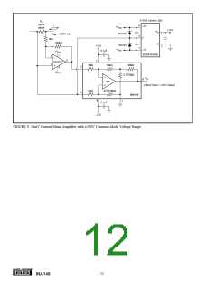
FIGURE 3. Preferred Offset Trim Circuit.
®
9
INA148

 BB [ BURR-BROWN CORPORATION ]