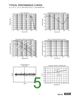
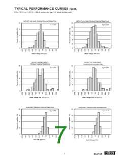
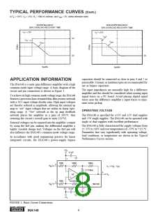
TYPICAL PERFORMANCE CURVES (Cont.)
At TA = +25°C, VS = ±15V, RL = 10kΩ to common, and VREF = 0V, unless otherwise noted.
INVERTING INPUT
NON-INVERTING INPUT
50% OVERLOAD RECOVERY TIME
50% OVERLOAD RECOVERY TIME
VS = ±15V
VS = ±15V
VIN
+
0V
0V
–
VIN
VOUT
VOUT
0V
5µs/div
5µs/div
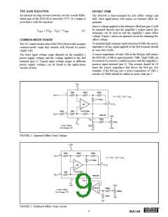
capacitors should be connected as close to pins 4 and 7 as
practicable. Ceramic or tantalum types are recommended for
use as bypass capacitors.
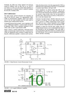
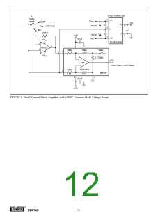
APPLICATION INFORMATION
The INA148 is a unity gain difference amplifier with a high
common-mode input voltage range. A basic diagram of the
circuit and pin connections is shown in Figure 1.
The input impedances are unusually high for a difference
amplifier and this should be considered when routing input
signal traces on a PC board. Avoid placing digital signal
traces near the difference amplifier’s input traces to mini-
mize noise pickup.
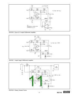
To achieve its high common-mode voltage range, the INA148
features a precision laser-trimmed thin-film resistor network
with a 20:1 input voltage divider ratio. High input voltages
are thereby reduced in amplitude, allowing the internal op
amp to “see” input voltages that are within its linear oper-
ating range. A “Tee” network in the op amp feedback
network places the amplifier in a gain of 20V/V, thus
restoring the circuit’s overall gain to unity (1V/V).
OPERATING VOLTAGE
The INA148 is specified for ±15V and ±5V dual supplies
and +5V single supplies. The INA148 can be operated with
single or dual supplies with excellent performance.
External voltages can be summed into the amplifier’s output
by using the Ref pin, making the differential amplifier a
highly versatile design tool. Voltages on the Ref pin will
also influence the INA148’s common-mode voltage range.
The INA148 is fully characterized for supply voltages from
±1.35V to ±18V and over temperatures of –55ºC to +125 ºC.
Parameters that vary significantly with operating voltage,
load conditions, or temperature are shown in the Typical
Performance Curves section.
In accordance with good engineering practice for linear
integrated circuits, the INA148’s power-supply bypass
+VS
0.1µF
7
1MΩ
1MΩ
50kΩ
50kΩ
2
3
VI–N
VO = (VI+N – VI–N
)
2.7778kΩ
6
VO
A1
52.6316kΩ
VI+N
INA148
4
1
0.1µF
–VS
FIGURE 1. Basic Circuit Connections.
®
8
INA148

 BB [ BURR-BROWN CORPORATION ]