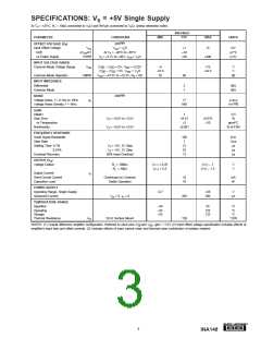
SPECIFICATIONS: VS = +5V Single Supply
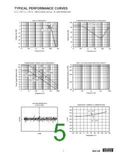
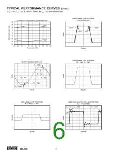
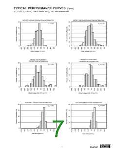
At TA = +25°C, RL = 10kΩ connected to VS/2 and Ref pin connected to VS/2, unless otherwise noted.
INA148UA
TYP
PARAMETER
CONDITIONS
MIN
MAX
UNITS
OFFSET VOLTAGE (VO)
Input Offset Voltage
Drift
RTI(1)(2)
VCM = VS/2
VOS
∆VOS/∆T
PSRR
±1
±5
mV
At TA = –40°C to +85°C
VS = +2.7V to +36V, VCM = VS/2
±10
±50
µV°C
µV/V
vs Power Supply
±400
INPUT VOLTAGE RANGE
Common-Mode Voltage Range
VCM
(VI+N) – (VI–N) = 0V, VREF = 0.25V
(VI+N) – (VI–N) = 0V, VREF = VS/2
VCM = –47.5V to +32.5V, RS = 0Ω
–4
–47.5
70
+75
V
V
+32.5
Common-Mode Rejection
CMRR
86
dB
INPUT IMPEDANCE
Differential
2
1
MΩ
MΩ
Common Mode
NOISE
RTI(1)(3)
Voltage Noise, f = 0.1Hz to 10Hz
Voltage Noise Density, f = 1kHz
en
17
µVp-p
880
nV/√Hz
GAIN
Initial(1)
Gain Error
1
V/V
%
V
O = +0.5V to +3.5V
±0.01
±0.075
±10
vs Temperature
Nonlinearity
±3
ppm/°C
VO = +0.5V to +3.5V
±0.001
% of FSR
FREQUENCY RESPONSE
Small Signal Bandwidth
Slew Rate
100
1
kHz
V/µs
µs
Settling Time: 0.1%
0.01%
VS = +5V, 3V Step
VS = +5V, 3V Step
50% Input Overload
21
25
13
µs
Overload Recovery
µs
OUTPUT (VO)
Voltage Output
RL = 100kΩ
RL = 10kΩ
(V–) + 0.25
(V–) + 0.5
(V+) – 1
V
V
(V+) – 1.5
Output Current
IO
Short-Circiuit Current
Capacitive Load
Continuous to Common
Stable Operation
±8
mA
nF
10
POWER SUPPLY
Operating Range, Single Supply
Quiescent Current
+2.7
+36
300
V
VIN = 0, IO = 0
260
µA
TEMPERATURE RANGE
Specified
–40
–55
–55
85
°C
°C
°C
Operating
Storage
125
125
Thermal Resistance
θJA
SO-8 Surface Mount
150
°C/W
NOTES: (1) Overall difference amplifier configuration. Referred to input pins (VI+N and VI–N), gain = 1V/V (2) Input offset voltage specification includes effects of
amplifier's input bias and offset currents. (3) Includes effects of input current noise and thermal noise contribution of resistor network.
®
3
INA148

 BB [ BURR-BROWN CORPORATION ]