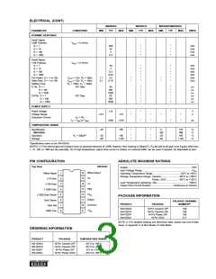
Other gains between 1 and 10, 10 and 100, and 100 and 1000
can also be obtained by connecting an external resistor
between pin 6 and either pin 2, 3, or 4, respectively (see
Figure 6 for application).
OPTIONAL FILTERING
The INA102 has provisions for accomplishing filtering with
one external capacitor between pins 11 and 13. This single-
pole filter can be used to reduce noise outside the signal
bandwidth, but with some degradation to AC CMR.
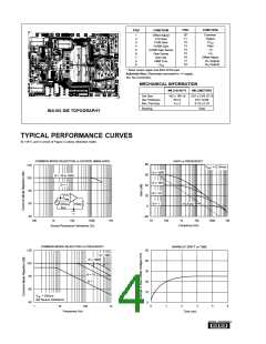
G = 1 + (40/RG) where RG is the total resistance between the
two inverting inputs of the input op amps. At high gains,
where the value of RG becomes small, additional resistance
(i.e., relays or sockets) in the RG circuit will contribute to a
gain error. Care should be taken to minimize this effect.
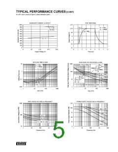
When it is important to preserve CMR versus frequency
(especially at 60Hz), two capacitors should be used. The
additional capacitor is connected between pins 8 and 10. This
will maintain a balance of impedances in the output stage.
Either of these capacitors could also be trimmed slightly, to
maximize CMR, if desired. Note that their ratio tracking will
affect CMR over temperature.
OPTIONAL OFFSET ADJUSTMENT PROCEDURE
It is sometimes desirable to null the input and/or output offset
to achieve higher accuracy. The quality of the potentiometer
will affect the results; therefore, choose one with good
temperature and mechanical-resistance stability.
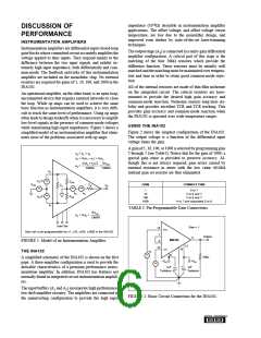
OPTIONAL COMMON-MODE REJECTION TRIM
The INA102 is laser-adjusted during manufacturing to assure
high CMR. However, if desired, a small resistance can be
added in series with pin 10 to trim the CMR to an improved
level. Depending upon the nature of the internal imbalances,
either positive or negative resistance value could be required.
The circuit shown in Figure 4 acts as a bipolar potentiometer
and allows easy adjustment of CMR.
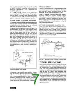
The optional offset null capabilities are shown in Figure 3. R4
adjustment affects only the input stage component of the
offset voltage. Note that the null condition will be disturbed
when the gain is changed. Also, the input drift will be
affected by approximately 0.31µV/°C per 100µV of input
offset voltage that is trimmed. Therefore, care should be
taken when considering use of the control for removal of
other sources of offset. Output offset correction can be
accomplished with A1, R1, R2, and R3, by applying a voltage
to Common (pin 10) through a buffer amplifier. This buffer
limits the resistance in series with pin 10 to minimize CMR
error. Resistance above 0.1Ω will cause the common-mode
rejection to fall below 100dB. Be certain to keep this resist-
ance low.
15
INA102
1kΩ
1kΩ
OPA177
1kΩ
14
eCM
10
~
Common
20Ω
CMR
Adjust
–VCC
1kΩ
Input Offset Adjust
R4
1
±15mV adjustment at the output.
100kΩ
INA102
10
Procedure:
1. Connect CMV to both inputs.
2. Adjust potentiometer for near zero at the output.
16
Output Offset
Adjust
+15VDC
R1
FIGURE 4. Optional Circuit for Externally Trimming CMR.
R3
A1
OPA27
100kΩ
1MΩ
TYPICAL APPLICATIONS
–15VDC
Many applications of instrumentation amplifiers involve the
amplification of low-level differential signals from bridges
and transducers such as strain gages, thermocouples, and
RTDs. Some of the important parameters include common-
mode rejection (differential cancellation of common-mode
offset and noise, see Figure 1), input impedance, offset
voltage and drift, gain accuracy, linearity, and noise. The
INA102 accomplishes all of these with high precision at
surprisingly low quiescent current. However, in higher gains
(>100), the bias current can cause a large offset error at the
output. This can saturate the output unless the source imped-
ance is separated, e.g., two 500kΩ paths instead of one 1MΩ
unbalanced input. Figures 5 through 16 show some typical
applications circuits.
R2
1kΩ
FIGURE 3. Optional Offset Nulling.
It is important to not exceed the input amplifiers’ dynamic
range. The amplified differential input signal and its associ-
ated common-mode voltage should not cause the output of
A1 or A2 to exceed approximately ±12V with ±15V supplies,
or nonlinear operation will result. To protect against mois-
ture, especially in high gain, sealing compound may be used.
Current injected into the offset pins should be minimized.
®

 BB [ BURR-BROWN CORPORATION ]