ABSOLUTE MAXIMUM RATINGS
+VA to AGND ........................................................................ –0.3V to +6V
+VD to DGND ........................................................................ –0.3V to +6V
AGND to DGND ................................................................. –0.3V to –0.3V
ELECTROSTATIC
DISCHARGE SENSITIVITY
This integrated circuit can be damaged by ESD. Texas Instru-
ments recommends that all integrated circuits be handled with
appropriate precautions. Failure to observe proper handling
and installation procedures can cause damage.
+VA to +VD ............................................................................... –6V to +6V
CLK, PD, WRT to DGND ........................................... –0.3V to VD + 0.3V
D0-D11 to DGND ....................................................... –0.3V to VD + 0.3V
IOUT, IOUT to AGND ........................................................ –1V to VA + 0.3V
GSET to AGND .......................................................... –0.3V to VA + 0.3V
REFIN, FSA to AGND ................................................. –0.3V to VA + 0.3V
Junction Temperature .................................................................... +150°C
Case Temperature ......................................................................... +100°C
Storage Temperature .................................................................... +125°C
ESD damage can range from subtle performance degradation
to complete device failure. Precision integrated circuits may
be more susceptible to damage because very small parametric
changes could cause the device not to meet its published
specifications.
PACKAGE/ORDERING INFORMATION
PACKAGE
SPECIFIED
DRAWING
NUMBER
PACKAGE
DESIGNATOR
TEMPERATURE
RANGE
PACKAGE
MARKING
ORDERING
NUMBER(1)
TRANSPORT
MEDIA
PRODUCT
PACKAGE
DAC2902Y
TQFP-48
355
48 PDF
–40°C to +85°C
DAC2902Y
DAC2902Y/250
DAC2902Y/2K
Tape and Reel
Tape and Reel
"
"
"
"
"
"
NOTE: (1) Models with a slash (/) are available only in Tape and Reel in the quantities indicated (e.g., /2K indicates 2000 devices per reel). Ordering 2000 pieces
of “DAC2902Y/2K” will get a single 2000-piece Tape and Reel.
PRODUCT
EVM ORDERING NUMBER
COMMENT
DAC2902
DAC2902-EVM
Fully populated evaluation board. See user manual for details.
ELECTRICAL CHARACTERISTICS
TMIN to TMAX, +VA = +5V, +VD = +3.3V, differential transformer coupled output, 50ý doubly-terminated, unless otherwise noted. Independant Gain Mode.
DAC2902Y
PARAMETER
RESOLUTION
CONDITIONS
MIN
TYP
MAX
UNITS
12
Bits
Output Update Rate (fCLOCK
)
125
MSPS
STATIC ACCURACY(1)
Differential Nonlinearity (DNL)
TA = +25°C
TMIN to TMAX
TA = +25°C
TMIN to TMAX
–2.0
–2.5
–2.0
–3.0
±1
±1
+2.0
+2.5
+2.0
+3.0
LSB
LSB
LSB
LSB
Integral Nonlinearity (INL)
DYNAMIC PERFORMANCE
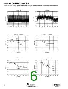
Spurious-Free Dynamic Range (SFDR)
fOUT = 1MHz, fCLOCK = 50MSPS
To Nyquist
0dBFS Output
–6dBFS Output
–12dBFS Output
72
82
77
72
81
81
81
77
dBc
dBc
dBc
dBc
dBc
dBc
dBc
fOUT = 1MHz, fCLOCK = 26MSPS
fOUT = 2.18MHz, fCLOCK = 52MSPS
fOUT = 5.24MHz, fCLOCK = 52MSPS
fOUT = 10.4MHz, fCLOCK = 78MSPS
fOUT = 15.7MHz, fCLOCK = 78MSPS
fOUT = 5.04MHz, fCLOCK = 100MSPS
fOUT = 20.2MHz, fCLOCK = 100MSPS
fOUT = 20.1MHz, fCLOCK = 125MSPS
71
80
70
72
dBc
dBc
dBc
dBc
fOUT = 40.2MHz, fCLOCK = 125MSPS
Spurious-Free Dynamic Range within a Window
fOUT = 1.0MHz, fCLOCK = 50MSPS
fOUT = 5.02MHz, fCLOCK = 50MSPS
fOUT = 5.03MHz, fCLOCK = 78MSPS
fOUT = 5.04MHz, fCLOCK = 125MSPS
Total Harmonic Distortion (THD)
64
dBc
2MHz Span
10MHz Span
10MHz Span
10MHz Span
80
90
88
88
88
dBc
dBc
dBc
dBc
fOUT = 1MHz, fCLOCK = 50MSPS
–79
–77
–76
–75
–70
dBc
dBc
dBc
dBc
fOUT = 5.02MHz, fCLOCK = 50MSPS
fOUT = 5.03MHz, fCLOCK = 78MSPS
fOUT = 5.04MHz, fCLOCK = 125MSPS
Multitone Power Ratio
8 Tone with 110kHz Spacing
0dBFS Output
fOUT = 2.0MHz to 2.99MHz, fCLOCK = 65MSPS
80
dBc
DAC2902
SBAS167A
2

 BB [ BURR-BROWN CORPORATION ]