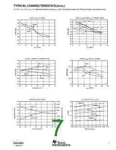
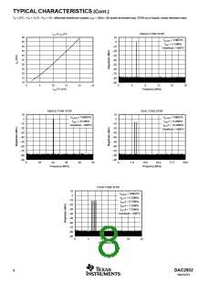
ELECTRICAL CHARACTERISTICS (Cont.)
TMIN to TMAX, +VA = +5V, +VD = +3.3V, differential transformer coupled output, 50ý doubly terminated, unless otherwise noted. Independant Gain Mode.
DAC2902Y
PARAMETER
CONDITIONS
MIN
TYP
MAX
UNITS
DYNAMIC PERFORMANCE (Cont.)
Signal-to-Noise Ratio (SNR)
fOUT = 5.02MHz, fCLOCK = 50MHz
Signal-to-Noise and Distortion (SINAD)
fOUT = 5.02MHz, fCLOCK = 50MHz
Channel Isolation
0dBFS Output
0dBFS Output
68
67
dBc
dBc
fOUT = 1MHz, fCLOCK = 52MSPS
fOUT = 20MHz, fCLOCK = 125MSPS
Output Settling Time(2)
Output Rise Time(2)
Output Fall Time(2)
85
77
30
2
dBc
dBc
ns
to 0.1%
10% to 90%
10% to 90%
ns
2
ns
Glitch Impulse
2
pV-s
DC ACCURACY
Full-Scale Output Range(3)(FSR)
Output Compliance Range
Gain Error—Full-Scale
Gain Error
All Bits HIGH, IOUT
2
20
+1.25
+5
mA
V
–1.0
–5
With Internal Reference
With External Reference
With Internal Reference
With Internal Reference
With Internal Reference
With Internal Reference
+5V, ±10%
±1
±1
%FSR
%FSR
%FSR
ppmFSR/°C
%FSR
ppmFSR/°C
%FSR/V
%FSR/V
pA/ Hz
pA/šHz
kΩ
–2.5
–2.0
+2.5
+2.0
Gain Matching
0.5
±50
Gain Drift
Offset Error
–0.02
+0.02
Offset Drift
±0.2
Power-Supply Rejection, +VA
Power-Supply Rejection, +VD
Output Noise
–0.2
+0.2
+3.3V, ±10%
–0.025
+0.025
IOUT = 20mA, RLOAD = 50Ω
IOUT = 2mA
50
30
200
6
Output Resistance
Output Capacitance
IOUT, IOUT to Ground
pF
REFERENCE/CONTROL AMP
Reference Voltage
+1.18
+0.5
+1.25
±50
100
0.3
+1.31
+1.25
V
Reference Voltage Drift
ppmFSR/°C
Reference Output Current
Reference Multiplying Bandwidth
Input Compliance Range
nA
MHz
V
DIGITAL INPUTS
Logic Coding
Straight Binary
Logic High Voltage, VIH
Logic Low Voltage, VIL
Logic High Voltage, VIH
Logic Low Voltage, VIL
+VD = +5V
+VD = +5V
+VD = 3.3V
+VD = 3.3V
+VD = 3.3V
+VD = 3.3V
3.5
2
5
0
V
V
1.2
0.8
3
V
0
V
(4)
Logic High Current, IIH
±10
±10
5
µA
µA
pF
Logic Low Current
Input Capacitance
POWER SUPPLY
Supply Voltages
+VA
+3.0
+3.0
+5
+5.5
+5.5
V
V
+VD
+3.3
Supply Current
(5)
IVA
VA = +5V, lOUT = 20mA
Power-Down Mode
59
1.7
64
3
mA
mA
(5)
IVA
(5)
IVD
4.2
7
mA
(6)
IVD
15.5
310
345
130
23
18
345
380
mA
Power Dissipation(5)
Power Dissipation(6)
Power Dissipation(5)
Power Dissipation
Thermal Resistance, TQFP-48
θJA
VA = +5V, VD = 3.3V, lOUT = 20mA
VA = +5V, VD = 3.3V, lOUT = 20mA
VA = +5V, VD = 3.3V, lOUT = 2mA
Power-Down Mode
mW
mW
mW
mW
38
60
13
°C/W
°C/W
θJC
TEMPERATURE RANGE
Specified
Ambient
Ambient
–40
–40
+85
+85
°C
°C
Operating
NOTES: (1) At output lOUT, while driving a virtual ground. (2) Measured single-ended into 50ý load. (3) Nominal full-scale output current is 32 • IREF; see Application
section for details. (4) Typically 45µA for the PD pin, which has an internal pull-down resistor. (5) Measured at fCLOCK = 25MSPS and fOUT = 1MHz. (6) Measured
at fCLOCK = 100MSPS and fOUT = 40MHz.
DAC2902
SBAS167A
3

 BB [ BURR-BROWN CORPORATION ]