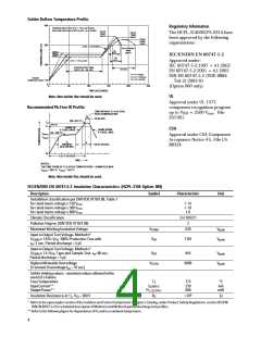
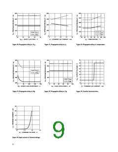
Solder Reflow Temperature Profile
300
Regulatory Information
PREHEATING RATE 3°C + 1°C/–0.5°C/SEC.
REFLOW HEATING RATE 2.5°C ± 0.5°C/SEC.
PEAK
TEMP.
245°C
PEAK
TEMP.
240°C
The HCPL-3140/HCPL-0314 have
been approved by the following
organizations:
PEAK
TEMP.
230°C
200
2.5°C ± 0.5°C/SEC.
SOLDERING
TIME
200°C
30
160°C
150°C
140°C
SEC.
IEC/EN/DIN EN 60747-5-2
30
SEC.
3°C + 1°C/–0.5°C
Approved under :
100
IEC 60747-5-2:1997 + A1:2002
EN 60747-5-2:2001 + A1:2002
DIN EN 60747-5-2 (VDE 0884
Teil 2):2003-01
PREHEATING TIME
150°C, 90 + 30 SEC.
50 SEC.
TIGHT
TYPICAL
LOOSE
ROOM
TEMPERATURE
0
0
50
100
150
200
250
(Option 060 only)
TIME (SECONDS)
UL
Note: Non-halide flux should be used.
Approval under UL 1577,
Recommended Pb-Free IR Profile
component recognition program
TIME WITHIN 5 °C of ACTUAL
PEAKTEMPERATURE
up to V = 2500 V . File
ISO
rms
t
p
E55361.
20-40 SEC.
260 +0/-5 °C
T
T
p
217 °C
L
RAMP-UP
3 °C/SEC. MAX.
CSA
RAMP-DOWN
6 °C/SEC. MAX.
150 - 200 °C
T
smax
Approval under CSA Component
Acceptance Notice # 5, File CA
88324.
T
smin
t
s
t
L
60 to 150 SEC.
PREHEAT
60 to 180 SEC.
25
t 25 °C to PEAK
TIME
NOTES:
THE TIME FROM 25 °C to PEAK TEMPERATURE = 8 MINUTES MAX.
= 200 °C, = 150 °C
T
T
smin
smax
Note: Non-halide flux should be used.
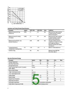
IEC/EN/DIN EN 60747-5-2 Insulation Characteristics (HCPL-3140 Option 060)
Description
Symbol
Characteristic
Unit
Installation classification per DIN VDE 0110/1.89, Table 1
for rated mains voltage ≤ 150 V
I - IV
I - III
I-II
rms
for rated mains voltage ≤ 300 V
rms
for rated mains voltage ≤ 600 V
rms
Climatic Classification
55/100/21
Pollution Degree (DIN VDE 0110/1.89)
MaximumWorking Insulation Voltage
Input to Output Test Voltage, Method b*
2
V
630
V
peak
IORM
V
IORM x 1.875=V , 100% Production Test with
V
1181
V
peak
PR
PR
tm=1 sec, Partial discharge < 5 pC
Input to Output Test Voltage, Method a*
V
IORM x 1.5=V , Type and Sample Test, tm=60 sec,
V
PR
945
V
peak
PR
Partial discharge < 5 pC
HighestAllowable Overvoltage
V
IOTM
6000
V
peak
(Transient Overvoltage tini = 10 sec)
Safety-limiting values - maximum values allowed in the
event of a failure.
Case Temperature
InputCurrent**
OutputPower**
TS
175
230
600
°C
mA
mW
IS,INPUT
PS,OUTPUT
Insulation Resistance at TS, V = 500 V
RS
>109
Ω
IO
* Refer to the optocoupler section of the Isolation and Control Components Designer’s Catalog, under Product Safety Regulations section IEC/EN/
DIN EN 60747-5-2 for a detailed description of Method a and Method b partial discharge test profiles.
** Refer to the following figure for dependence of P and I on ambient temperature.
S
S
4

 AVAGO [ AVAGO TECHNOLOGIES LIMITED ]