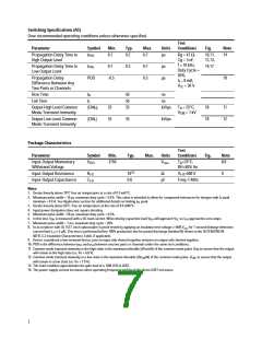
Switching Specifications (AC)
Over recommended operating conditions unless otherwise specified.
Test
Parameter
Symbol
Min.
Typ.
Max.
Units
Conditions
Fig.
Note
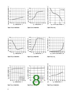
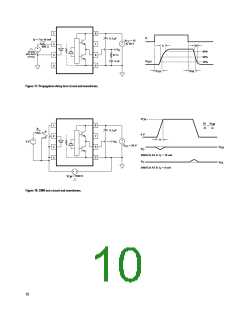
Propagation Delay Time to
High Output Level
t
0.1
0.2
0.7
µs
Rg = 47 Ω,
Cg = 3 nF,
f = 10 kHz,
Duty Cycle =
50%,
10,11,
12,13,
14
PLH
Propagation Delay Time to
Low Output Level
t
0.1
0.3
0.7
0.5
µs
µs
14,17
PHL
Propagation Delay
Difference Between Any
Two Parts or Channels
PDD
-0.5
10
I
F =
8 mA,
V = 30 V
CC
Rise Time
Fall Time
t
t
50
50
35
ns
R
F
ns
Output High Level Common
Mode Transient Immunity
|CM |
25
25
kV/µs
T = 25°C,
18
18
11
12
H
A
V
= 1 kV
CM
Output Low Level Common
Mode Transient Immunity
|CM |
35
kV/µs
L
Package Characteristics
Parameter
Test
Conditions
Symbol
Min.
Typ.
Max.
Units
Fig.
Note
Input-Output Momentary
Withstand Voltage
V
ISO
3750
V
rms
T =25°C,
RH<50% for
8,9
A
12
Input-Output Resistance
Input-Output Capacitance
R
10
0.6
Ω
V =500 V
9
I-O
I-O
C
I-O
pF
Freq=1 MHz
Notes:
1. Derate linearly above 70°C free air temperature at a rate of 0.3 mA/°C.
2. Maximum pulse width = 10 µs, maximum duty cycle = 0.2%. This value is intended to allow for component tolerances for designs with I peak
O
minimum = 0.4 A. See Application section for additional details on limiting I peak.
OL
3. Derate linearly above 85°C, free air temperature at the rate of 4.0 mW/°C.
4. Input power dissipation does not require derating.
5. Maximum pulse width = 50 µs, maximum duty cycle = 0.5%.
6. In this test, V is measured with a DC load current. When driving capacitive load V will approach V as I approaches zero amps.
OH
OH
CC
OH
7. Maximum pulse width = 1 ms, maximum duty cycle = 20%.
8. In accordance with UL 1577, each optocoupler is proof tested by applying an insulation test voltage ≥ 4500 Vrms for 1 second (leakage detection
current limit I ≤ 5 µA). This test is performed before 100% production test for partial discharge (method B) shown in the IEC/EN/DIN EN
I-O
60747-5-2 Insulation Characteristics Table, if applicable.
9. Device considered a two-terminal device: pins on input side shorted together and pins on output side shorted together.
10. PDD is the difference between t
and t
between any two parts or channels under the same test conditions.
PLH
PHL
11. Common mode transient immunity in the high state is the maximum tolerable |dVcm/dt| of the common mode pulse V to assure that the output
CM
will remain in the high state (i.e. Vo > 6.0 V).
12. Common mode transient immunity in a low state is the maximum tolerable |dV /dt| of the common mode pulse, V , to assure that the output
CM
CM
will remain in a low state (i.e. Vo < 1.0 V).
13. This load condition approximates the gate load of a 1200 V/25 A IGBT.
14. The power supply current increases when operating frequency and Qg of the driven IGBT increases.
7

 AVAGO [ AVAGO TECHNOLOGIES LIMITED ]