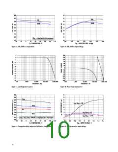
Shunt Resistor Connections
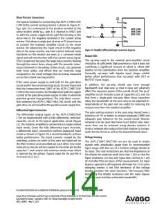
5 V
The typical method for connecting the ACPL-C79B/C79A/
C790 to the current sensing resistor is shown in Figure 2±.
VDD1
VIN+
Ra
Rb
+Input
–Input
V + (pin 2) is connected to the positive terminal of the
IN
ACPL-C79B/
ACPL-C79A/
ACPL-C790
sense resistor, while V – (pin ꢀ) is shorted to GND± (pin
C
IN
4), with the power-supply return path functioning as the
sense line to the negative terminal of the current sense
resistor. This allows a single pair of wires or PC board traces
to connect the isolation amplifier circuit to the sense
resistor. By referencing the input circuit to the negative
side of the sense resistor, any load current induced noise
transients on the resistor are seen as a common-mode
signal and will not interfere with the current-sense signal.
This is important because the large load currents flowing
through the motor drive, along with the parasitic induc-
tances inherent in the wiring of the circuit, can generate
both noise spikes and offsets that are relatively large
compared to the small voltages that are being measured
across the current sensing resistor.
VIN
–
GND1
Figure 24. Simplified differential input connection diagram.
Output Side
The op-amp used in the external post-amplifier circuit
should be of sufficiently high precision so that it does not
contribute a significant amount of offset or offset drift
relative to the contribution from the isolation amplifier.
Generally, op-amps with bipolar input stages exhibit
better offset performance than op-amps with JFET or
MOSFET input stages.
If the same power supply is used both for the gate drive
circuit and for the current sensing circuit, it is very important
that the connection from GND± of the ACPL-C79B/C79A/
C790 to the sense resistor be the only return path for supply
current to the gate drive power supply in order to eliminate
potential ground loop problems. The only direct connec-
tion between the ACPL-C79B/C79A/C790 circuit and the
gate drive circuit should be the positive power supply line.
In addition, the op-amp should also have enough
bandwidth and slew rate so that it does not adversely
affect the response speed of the overall circuit. The post-
amplifier circuit includes a pair of capacitors (Cꢁ and C6)
that form a single-pole low-pass filter; these capacitors
allow the bandwidth of the post-amp to be adjusted in-
dependently of the gain and are useful for reducing the
output noise from the isolation amplifier.
Differential Input Connection
The gain-setting resistors in the post-amp should have a
tolerance of ±1 or better to ensure adequate CMRR and
adequate gain tolerance for the overall circuit. Resistor
networks can be used that have much better ratio toler-
ances than can be achieved using discrete resistors. A
resistor network also reduces the total number of compo-
nents for the circuit as well as the required board space.
The differential analog inputs of the ACPL-C79B/C79A/
C790 are implemented with a fully-differential, switched-
capacitor circuit. In the typical application circuit (Figure
2±), the isolation amplifier is connected in a single-ended
input mode. Given the fully differential input structure,
a differential input connection method (balanced input
mode as shown in Figure 24) is recommended to achieve
better performance. The input currents created by the
switching actions on both of the pins are balanced on
the filter resistors and cancelled out each other. Any noise
induced on one pin will be coupled to the other pin by the
capacitor C and creates only common mode noise which
is rejected by the device. Typical value for Ra and Rb is
±0 Ω and 22 nF for C.
Voltage Sensing
The ACPL-C79B/C79A/C790 can also be used to isolate
signals with amplitudes larger than its recommended
input range with the use of a resistive voltage divider at
its input. The only restrictions are that the impedance of
the divider be relatively small (less than ± kΩ) so that the
input resistance (22 kΩ) and input bias current (0.± µA)
do not affect the accuracy of the measurement. An input
bypass capacitor is still required, although the ±0 Ω series
damping resistor is not (the resistance of the voltage
divider provides the same function). The low-pass filter
formed by the divider resistance and the input bypass
capacitor may limit the achievable bandwidth.
For product information and a complete list of distributors, please go to our web site: www.avagotech.com
Avago, Avago Technologies, and the A logo are trademarks of Avago Technologies in the United States and other countries.
Data subject to change. Copyright © 2005-2013 Avago Technologies. All rights reserved.
AV02-2460EN - May 13, 2013

 AVAGO [ AVAGO TECHNOLOGIES LIMITED ]