Application Information
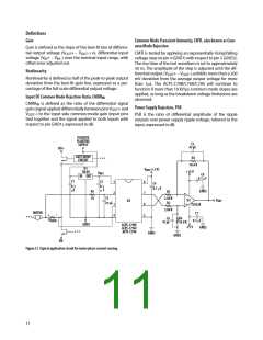
Application Circuit
The typical application circuit is shown in Figure 2±. A
floating power supply (which in many applications could
be the same supply that is used to drive the high-side
power transistor) is regulated to ꢁ V using a simple three-
terminal voltage regulator (U±). The voltage from the
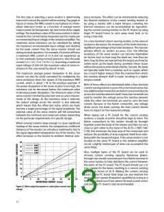
PC Board Layout
The design of the printed circuit board (PCB) should follow
good layout practices, such as keeping bypass capacitors
close to the supply pins, keeping output signals away from
input signals, the use of ground and power planes, etc. In
addition, the layout of the PCB can also affect the isolation
transient immunity (CMTI) of the ACPL-C79B/C79A/C790,
due primarily to stray capacitive coupling between the
input and the output circuits. To obtain optimal CMTI
performance, the layout of the PC board should minimize
any stray coupling by maintaining the maximum possible
distance between the input and output sides of the circuit
and ensuring that any ground or power plane on the PC
board does not pass directly below or extend much wider
than the body of the ACPL-C79B/C79A/C790. Figure 22
shows an example PCB layout.
current sensing resistor, or shunt (R
), is applied to
SENSE
the input of the ACPL-C79B/C79A/C790 through an RC
anti-aliasing filter (Rꢁ and Cꢀ). And finally, the differential
output of the isolation amplifier is converted to a ground-
referenced single-ended output voltage with a simple
differential amplifier circuit (Uꢀ and associated com-
ponents). Although the application circuit is relatively
simple, a few recommendations should be followed to
ensure optimal performance.
Power Supplies and Bypassing
As mentioned above, an inexpensive 78L0ꢁ three-terminal
regulator can be used to reduce the gate-drive power
supply voltage to ꢁ V. To help attenuate high frequency
power supply noise or ripple, a resistor or inductor can
be used in series with the input of the regulator to form a
low-pass filter with the regulator’s input bypass capacitor.
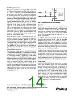
TO GND1 TO VDD1
C2
TO VDD2 TO GND2
C4
U2
TO RSENSE+
VOUT+
VOUT–
R5
C3
The power supply for the isolation amplifier is most
often obtained from the same supply used to power the
power transistor gate drive circuit. If a dedicated supply
is required, in many cases it is possible to add an addi-
tional winding on an existing transformer. Otherwise,
some sort of simple isolated supply can be used, such as
a line powered transformer or a high-frequency DC-DC
converter.
TO RSENSE–
ACPL-C79B/C79A/C790
Note: Drawing not to scale
Figure 22. Example printed circuit board layout.
Shunt Resistor Selection
The current sensing resistor should have low resistance (to
minimize power dissipation), low inductance (to minimize
di/dt induced voltage spikes which could adversely
affect operation), and reasonable tolerance (to maintain
overall circuit accuracy). Choosing a particular value for
the resistor is usually a compromise between minimiz-
ing power dissipation and maximizing accuracy. Smaller
sense resistance decreases power dissipation, while larger
sense resistance can improve circuit accuracy by utilizing
the full input range of the ACPL-C79B/C79A/C790.
As shown in Figure 2±, 0.± µF bypass capacitors (C2, C4)
should be located as close as possible to the pins of the
isolation amplifier. The bypass capacitors are required
because of the high-speed digital nature of the signals
inside the isolation amplifier. A 47 nF bypass capacitor
(Cꢀ) is also recommended at the input pins due to the
switched-capacitor nature of the input circuit. The input
bypass capacitor also forms part of the anti-aliasing filter,
which is recommended to prevent high-frequency noise
from aliasing down to lower frequencies and interfering
with the input signal. The input filter also performs an
important reliability function – it reduces transient spikes
from ESD events flowing through the current sensing
resistor.
±2

 AVAGO [ AVAGO TECHNOLOGIES LIMITED ]