AT90CAN128
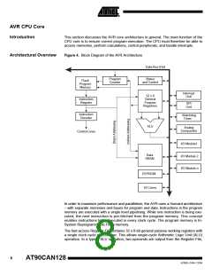
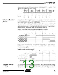
the operation is executed, and the result is stored back in the Register File – in one
clock cycle.
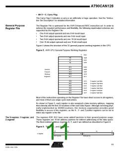
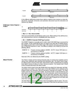
Six of the 32 registers can be used as three 16-bit indirect address register pointers for
Data Space addressing – enabling efficient address calculations. One of the these
address pointers can also be used as an address pointer for look up tables in Flash pro-
gram memory. These added function registers are the 16-bit X-, Y-, and Z-register,
described later in this section.
The ALU supports arithmetic and logic operations between registers or between a con-
stant and a register. Single register operations can also be executed in the ALU. After
an arithmetic operation, the Status Register is updated to reflect information about the
result of the operation.
Program flow is provided by conditional and unconditional jump and call instructions,
able to directly address the whole address space. Most AVR instructions have a single
16-bit word format. Every program memory address contains a 16- or 32-bit instruction.
Program Flash memory space is divided in two sections, the Boot Program section and
the Application Program section. Both sections have dedicated Lock bits for write and
read/write protection. The SPM (Store Program Memory) instruction that writes into the
Application Flash memory section must reside in the Boot Program section.
During interrupts and subroutine calls, the return address Program Counter (PC) is
stored on the Stack. The Stack is effectively allocated in the general data SRAM, and
consequently the Stack size is only limited by the total SRAM size and the usage of the
SRAM. All user programs must initialize the SP in the Reset routine (before subroutines
or interrupts are executed). The Stack Pointer (SP) is read/write accessible in the I/O
space. The data SRAM can easily be accessed through the five different addressing
modes supported in the AVR architecture.
The memory spaces in the AVR architecture are all linear and regular memory maps.
A flexible interrupt module has its control registers in the I/O space with an additional
Global Interrupt Enable bit in the Status Register. All interrupts have a separate Interrupt
Vector in the Interrupt Vector table. The interrupts have priority in accordance with their
Interrupt Vector position. The lower the Interrupt Vector address, the higher is the
priority.
The I/O memory space contains 64 addresses for CPU peripheral functions as Control
Registers, SPI, and other I/O functions. The I/O Memory can be accessed directly, or as
the Data Space locations following those of the Register File, 0x20 - 0x5F. In addition,
the AT90CAN128 has Extended I/O space from 0x60 - 0xFF in SRAM where only the
ST/STS/STD and LD/LDS/LDD instructions can be used.
ALU – Arithmetic Logic
Unit
The high-performance AVR ALU operates in direct connection with all the 32 general
purpose working registers. Within a single clock cycle, arithmetic operations between
general purpose registers or between a register and an immediate are executed. The
ALU operations are divided into three main categories – arithmetic, logical, and bit-func-
tions. Some implementations of the architecture also provide a powerful multiplier
supporting both signed/unsigned multiplication and fractional format. See the “Instruc-
tion Set” section for a detailed description.
9
4250E–CAN–12/04

 ATMEL [ ATMEL ]