AVR CPU Core
Introduction
This section discusses the AVR core architecture in general. The main function of the
CPU core is to ensure correct program execution. The CPU must therefore be able to
access memories, perform calculations, control peripherals, and handle interrupts.
Architectural Overview
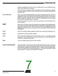
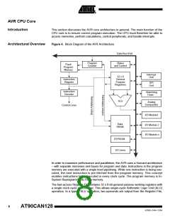
Figure 4. Block Diagram of the AVR Architecture
Data Bus 8-bit
Program
Counter
Status
and Control
Flash
Program
Memory
Interrupt
Unit
32 x 8
General
Purpose
Registrers
Instruction
Register
SPI
Unit
Instruction
Decoder
Watchdog
Timer
ALU
Analog
Comparator
Control Lines
I/O Module1
I/O Module 2
I/O Module n
Data
SRAM
EEPROM
I/O Lines
In order to maximize performance and parallelism, the AVR uses a Harvard architecture
– with separate memories and buses for program and data. Instructions in the program
memory are executed with a single level pipelining. While one instruction is being exe-
cuted, the next instruction is pre-fetched from the program memory. This concept
enables instructions to be executed in every clock cycle. The program memory is In-
System Reprogrammable Flash memory.
The fast-access Register File contains 32 x 8-bit general purpose working registers with
a single clock cycle access time. This allows single-cycle Arithmetic Logic Unit (ALU)
operation. In a typical ALU operation, two operands are output from the Register File,
8
AT90CAN128
4250E–CAN–12/04

 ATMEL [ ATMEL ]