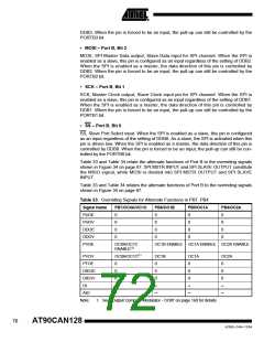
• TXCAN/XCK1 – Port D, Bit 5
TXCAN, CAN Transmit Data (Data output pin for the CAN). When the CAN is enabled,
this pin is configured as an output regardless of the value of DDD5.
XCK1, USART1 External clock. The Data Direction Register (DDD5) controls whether
the clock is output (DDD5 set) or input (DDD45 cleared). The XCK1 pin is active only
when the USART1 operates in Synchronous mode.
• ICP1 – Port D, Bit 4
ICP1, Input Capture Pin1. The PD4 pin can act as an input capture pin for
Timer/Counter1.
• INT3/TXD1 – Port D, Bit 3
INT3, External Interrupt source 3. The PD3 pin can serve as an external interrupt source
to the MCU.
TXD1, Transmit Data (Data output pin for the USART1). When the USART1 Transmitter
is enabled, this pin is configured as an output regardless of the value of DDD3.
• INT2/RXD1 – Port D, Bit 2
INT2, External Interrupt source 2. The PD2 pin can serve as an External Interrupt
source to the MCU.
RXD1, Receive Data (Data input pin for the USART1). When the USART1 receiver is
enabled this pin is configured as an input regardless of the value of DDD2. When the
USART forces this pin to be an input, the pull-up can still be controlled by the PORTD2
bit.
• INT1/SDA – Port D, Bit 1
INT1, External Interrupt source 1. The PD1 pin can serve as an external interrupt source
to the MCU.
SDA, Two-wire Serial Interface Data. When the TWEN bit in TWCR is set (one) to
enable the Two-wire Serial Interface, pin PD1 is disconnected from the port and
becomes the Serial Data I/O pin for the Two-wire Serial Interface. In this mode, there is
a spike filter on the pin to suppress spikes shorter than 50 ns on the input signal, and the
pin is driven by an open drain driver with slew-rate limitation.
• INT0/SCL – Port D, Bit 0
INT0, External Interrupt source 0. The PD0 pin can serve as an external interrupt source
to the MCU.
SCL, Two-wire Serial Interface Clock: When the TWEN bit in TWCR is set (one) to
enable the Two-wire Serial Interface, pin PD0 is disconnected from the port and
becomes the Serial Clock I/O pin for the Two-wire Serial Interface. In this mode, there is
a spike filter on the pin to suppress spikes shorter than 50 ns on the input signal, and the
pin is driven by an open drain driver with slew-rate limitation.
76
AT90CAN128
4250E–CAN–12/04

 ATMEL [ ATMEL ]