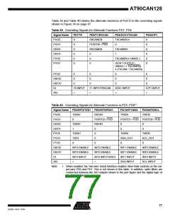
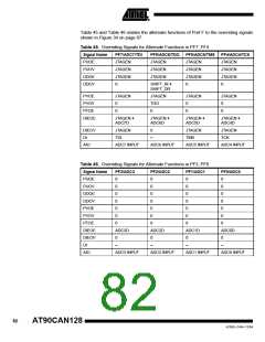
Table 43. Overriding Signals for Alternate Functions in PE3..PE0
Signal Name
PUOE
PUOV
DDOE
DDOV
PVOE
PVOV
PTOE
DIEOE
DIEOV
DI
PE3/AIN1/OC3A PE2/AIN0/XCK0 PE1/PDO/TXD0
PE0/PDI/RXD0
0
0
TXEN0
RXEN0
0
0
0
PORTE0 • PUD
0
0
TXEN0
RXEN0
0
0
1
0
OC3A ENABLE
UMSEL0
XCK0 OUTPUT
0
TXEN0
0
OC3A
TXD0
0
0
0
0
0
–
–
0
AIN1D(1)
AIN0D(1)
0
0
0
0
0
XCK0 INPUT
AIN0 INPUT
RXD0
AIO
AIN1 INPUT
–
Note:
1. AIN0D and AIN1D is described in “Digital Input Disable Register 1 – DIDR1” on page
264.
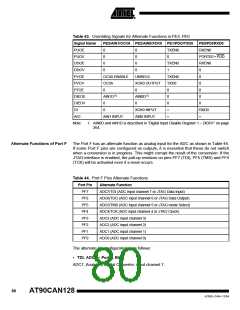
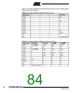
Alternate Functions of Port F
The Port F has an alternate function as analog input for the ADC as shown in Table 44.
If some Port F pins are configured as outputs, it is essential that these do not switch
when a conversion is in progress. This might corrupt the result of the conversion. If the
JTAG interface is enabled, the pull-up resistors on pins PF7 (TDI), PF5 (TMS) and PF4
(TCK) will be activated even if a reset occurs.
Table 44. Port F Pins Alternate Functions
Port Pin
PF7
Alternate Function
ADC7/TDI (ADC input channel 7 or JTAG Data Input)
ADC6/TDO (ADC input channel 6 or JTAG Data Output)
ADC5/TMS (ADC input channel 5 or JTAG mode Select)
ADC4/TCK (ADC input channel 4 or JTAG ClocK)
ADC3 (ADC input channel 3)
PF6
PF5
PF4
PF3
PF2
ADC2 (ADC input channel 2)
PF1
ADC1 (ADC input channel 1)
PF0
ADC0 (ADC input channel 0)
The alternate pin configuration is as follows:
• TDI, ADC7 – Port F, Bit 7
ADC7, Analog to Digital Converter, input channel 7
.
80
AT90CAN128
4250E–CAN–12/04

 ATMEL [ ATMEL ]